Data processor

Active Publication Date: 2011-07-21
RENESAS ELECTRONICS CORP
View PDF11 Cites 9 Cited by
  • Summary
  • Abstract
  • Description
  • Claims
  • Application Information

AI Technical Summary

Benefits of technology

In the embodiment, when the cache memory receives the spin wait request from the CPU, the cache memory temporarily stops outputting the acknowledge response to the read request from the CPU until the predetermined condition i

Problems solved by technology

Consequently, in a spin wait state, the processor and the cache memory operate at high speed and wait for release of a lock by another processor while consuming large power.
There is consequently a problem such that the processor consumes power vainly without performing any useful processes in the spin wait state.
However,

Method used


Image

  • Data processor
  • Data processor
  • Data processor

Examples


first embodiment

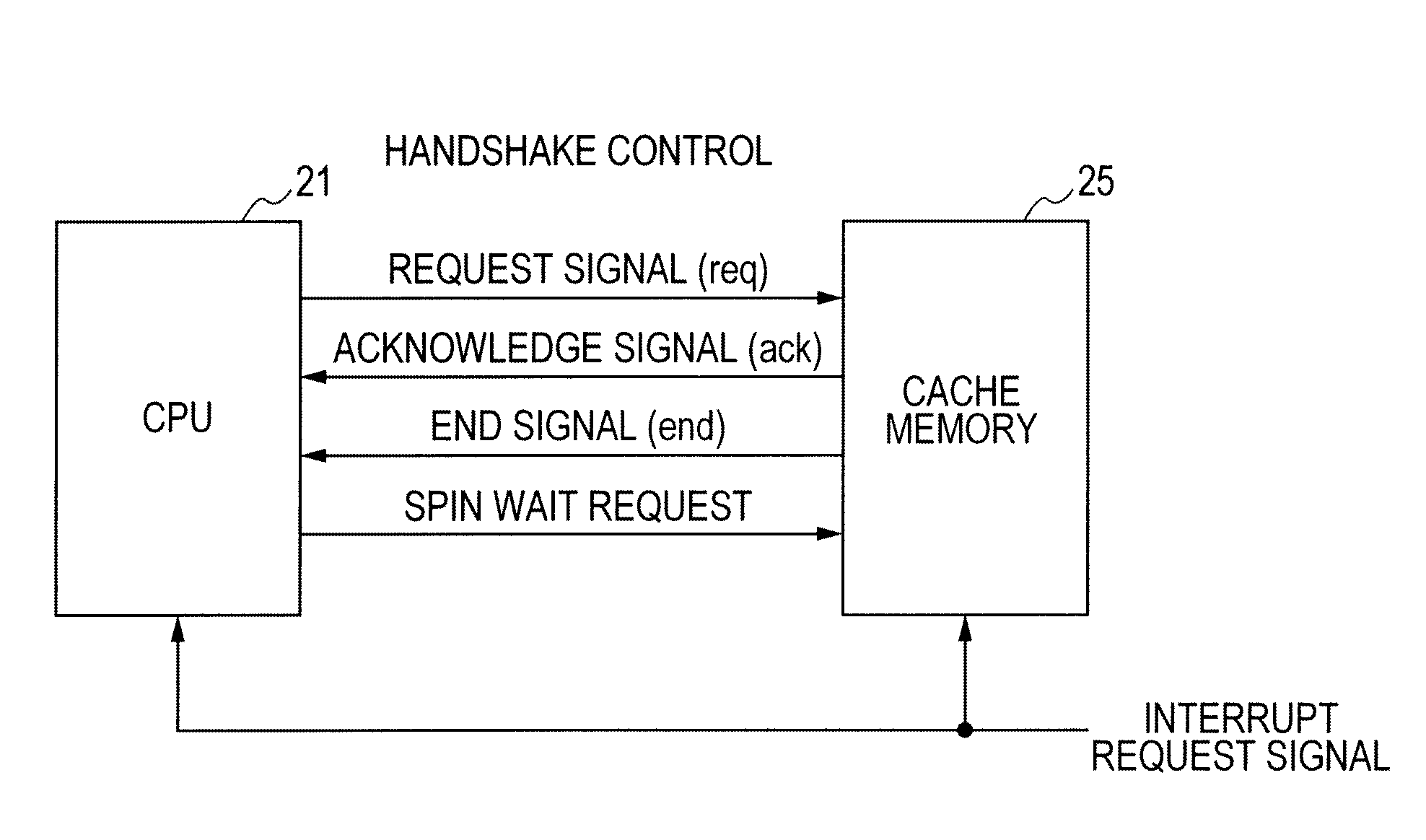
FIG. 6 is a diagram showing an example of connection between the CPU 21 and the cache memory 25 in the data processor according to the first embodiment of the invention. The CPU 21 and the cache memory 25 are coupled by handshake signals such as a request (req) signal, an acknowledge (ack) signal, and an end signal. By performing the handshake control by the CPU 21, a memory access process is performed with reliability.

The CPU 21 outputs a spin wait request signal to the cache memory 25 at the time of executing a weighted load instruction (LDS instruction) or a spin wait instruction (SPIN instruction) which will be described later. To the cache memory 25, an interrupt request signal is coupled. The details of them will be described later.

FIG. 7 is a block diagram showing a configuration example of the CPU 21 in the data processor in the first embodiment of the invention. The CPU 21 includes an instruction fetch unit 31, an instruction decode unit 32, a control unit 33, an address ge...

second embodiment

In the data processor in the first embodiment, when the CPU 21 executes the weighted load instruction, the CPU 21 transmits a spin wait request to the cache memory 25 to make the cache memory 25 enter the spin wait state. A data processor in a second embodiment is different from the data processor in the first embodiment only with respect to the point that a spin wait (SPIN) instruction is provided for the CPU 21, and the CPU 21 continuously holds the instruction until a load result becomes a designated value. Therefore, the detailed description of configurations and functions will not be repeated.

FIG. 17 is a diagram showing an example of a spinlock process code executed by the CPU 21 in the second embodiment of the invention. The spinlock process code is different from that of FIG. 10 only with respect to the point that a weighted load instruction (LDS instruction) and a bgtz instruction are replaced with a spin wait instruction (SPIN instruction).

The instruction is similar to the...

third embodiment

A data processor in a third embodiment of the invention is different from the data processors in the first and second embodiments only with respect to the point that a mode of supplying clocks to the CPU 21 and the cache memory 25 is changed interlockingly with shift to the spin wait state and return from the spin wait state. Therefore, the detailed description of configurations and functions will not be repeated.

FIG. 19 is a block diagram showing a configuration example of the data processor in the third embodiment of the invention. The data processor is obtained by adding a clock module (CLKC) 27 to the data processor in the first embodiment shown in FIG. 6.

The cache memory 25 is divided into a part which operates in a CPU clock domain and a part which operates in a cache clock domain. At the time of shift to the spin wait state, the cache memory 25 notifies the clock module 27 of the fact that the cache memory 25 is in the spin wait state and makes the clock module 27 perform clo...


PUM


Abstract

The present invention provides a data processor capable of reducing power consumption at the time of execution of a spin wait loop for a spinlock. A CPU executes a weighted load instruction at the time of performing a spinlock process and outputs a spin wait request to a corresponding cache memory. When the spin wait request is received from the CPU, the cache memory temporarily stops outputting an acknowledge response to a read request from the CPU until a predetermined condition (snoop write hit, interrupt request, or lapse of predetermined time) is satisfied. Therefore, pipeline execution of the CPU is stalled and the operation of the CPU and the cache memory can be temporarily stopped, and power consumption at the time of executing a spin wait loop can be reduced.

Description

CROSS-REFERENCE TO RELATED APPLICATIONSThe disclosure of Japanese Patent Application No. 2010-9234 filed on Jan. 19, 2010 including the specification, drawings and abstract is incorporated herein by reference in its entirety.BACKGROUND OF THE INVENTIONThe present invention relates to a spinlock method for interprocess exclusive control in a shared-memory multi-processor (multicore) system and, more particularly, relates to a multi-processor system realizing reduced power consumption in a spinlock operation by control of a cache memory.In recent years, a cache memory is often mounted on a microcomputer in order to increase processing speed. When a processor accesses a main storage via the cache memory, the processing speed at the time of a cache hit can be improved.In a multi-processor system including a plurality of such processors, the processors are connected to a common bus via cache memories and can access data in a common memory connected to the common bus.In a multi-processor,...

Claims


Application Information

Patent Timeline
IPC IPC(8): G06F12/08
CPCY02B60/1225G06F12/0831Y02D10/00
Inventor TAKATA, HIROKAZU
Owner RENESAS ELECTRONICS CORP
Why Eureka
Try Eureka