Organic Electronic Devices and Methods of Making the Same Using Solution Processing Techniques

a technology of organic electronic devices and processing techniques, which is applied in the direction of solid-state devices, electric lighting sources, and light sources, can solve the problems of increasing time, complexity and expense in the manufacturing process, reducing the robustness and lifetime of organic electronic devices, and reducing the wettability.

Inactive Publication Date: 2011-07-28
CAMBRIDGE DISPLAY TECH LTD
View PDF12 Cites 29 Cited by
  • Summary
  • Abstract
  • Description
  • Claims
  • Application Information

AI Technical Summary

Benefits of technology

[0063]According to preferred embodiments, the well-defining structure is for active organic material to be deposited over an electronic substrate comprising circuit elements, as other methods of decreasing wettability such as plasma treatments have been found to damage the underlying electronic circuitry of the substrate exposed in the wells.

Problems solved by technology

The double bank well-defining structure requires two deposition steps to form the first and second layers thus increasing time, complexity and expense in the manufacturing process when compared to a single bank well-defining structure.
Furthermore, the present applicant has found that there can be poor adhesion between the two layers of material in the double bank structure.
This is due to the non-stick properties of the low-wettability materials used for the second layer and can lead to delamination of the layers reducing the robustness and lifetime of the organic electronic device.
However, this requires yet another deposition step thus increasing time, complexity and expense in the manufacturing process yet further.

Method used


Image

  • Organic Electronic Devices and Methods of Making the Same Using Solution Processing Techniques
  • Organic Electronic Devices and Methods of Making the Same Using Solution Processing Techniques
  • Organic Electronic Devices and Methods of Making the Same Using Solution Processing Techniques

Examples


Embodiment Construction

[0081]Embodiments of the present invention relate to printed organic electronic devices which comprise a patterned well-defining bank structure. Embodiments seek to provide a bank structure in which the side walls of the wells are wetting whereas the top of the bank structure is anti wetting. Embodiments also seek to provide a manufacturing process that involves no plasma processes using fluorine based gas systems which have been found to damage circuitry elements or device layers exposed in the wells. Embodiments have the potential for obtaining good device performance whilst retaining optimum printing performance during deposition of the active organic material of the device from solution.

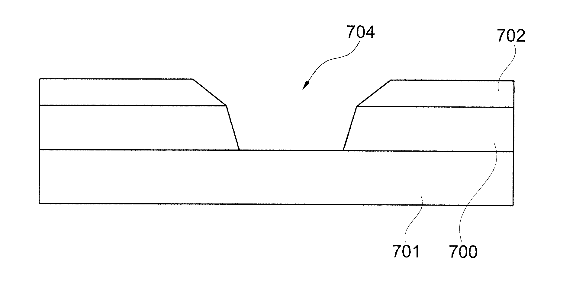
[0082]FIG. 7 shows a well-defining structure according to an embodiment of the present invention. The well-defining structure is disposed on an electronic substrate 701 and comprises a lower portion 700 of wettable material and an upper portion 702 of an inherently low wettability (high contact a...


PUM

PropertyMeasurementUnit
contact angleaaaaaaaaaa
contact anglesaaaaaaaaaa
contact angleaaaaaaaaaa

Abstract

A method of manufacturing an organic electronic device, the method comprising: providing a substrate; forming a well-defining structure over the substrate; and depositing a solution of organic semiconductive material and/or organic conductive material in wells defined by the well-defining structure, wherein the well-defining structure is formed by depositing a solution comprising a mixture of a first insulating material and a second insulating material, the second insulating material having a lower wettability than the first insulating material, and allowing the first and second insulating materials to at least partially phase separate wherein the second insulating material phase separates in a direction away from the substrate.

Description

FIELD OF INVENTION[0001]The present invention relates to organic electronic devices and methods of making the same using solution processing techniques. Particular embodiments of the present invention relate to organic thin film transistors, organic optoelectronic devices, organic light emissive display devices and methods of making the same using solution processing techniques.BACKGROUND OF THE INVENTION[0002]Methods of manufacturing organic electronic devices involving depositing active organic components from solution are known in the art. Such methods involve the preparation of a substrate onto which one or more active organic components can be deposited. If active organic components are deposited from solution, one problem is how to contain the active organic components in desired areas of the substrate. One solution to this problem is to provide a substrate comprising a patterned bank layer defining wells in which the active organic components can be deposited in solution. The...

Claims


Application Information

Patent Timeline
Patent Type & Authority Applications(United States)
IPC IPC(8): H01L29/06H01L21/36
CPCH01L27/3246H01L51/0545H01L51/0012H10K59/122H10K71/191H10K10/466H05B33/10H10K50/84H10K71/00
Inventor MCCONNELL, ANGELA
Owner CAMBRIDGE DISPLAY TECH LTD
Why Eureka
Try Eureka