Solid-state imaging device and electronic apparatus

a solid-state imaging and electronic equipment technology, applied in the direction of radioation control devices, television systems, television system scanning details, etc., can solve the problem of difficult to reduce the size of pixels, and achieve the effect of high reliability and high quality

Active Publication Date: 2011-07-28
SONY CORP
View PDF22 Cites 85 Cited by
  • Summary
  • Abstract
  • Description
  • Claims
  • Application Information

AI Technical Summary

Benefits of technology

[0029]According to the solid-state imaging device of the embodiment of the present invention, in the solid-state imaging device having shared pixels, it is possible to provide a solid-state imaging device having shared pixels between which a difference in sensitivity hardly occurs.
[0030]Accordi...

Problems solved by technology

Since the photodiodes and the plurality of pixel transistors are nec...

Method used


Image

  • Solid-state imaging device and electronic apparatus
  • Solid-state imaging device and electronic apparatus
  • Solid-state imaging device and electronic apparatus

Examples


first embodiment

3. First Embodiment

Configuration Example of Solid-State Imaging Device

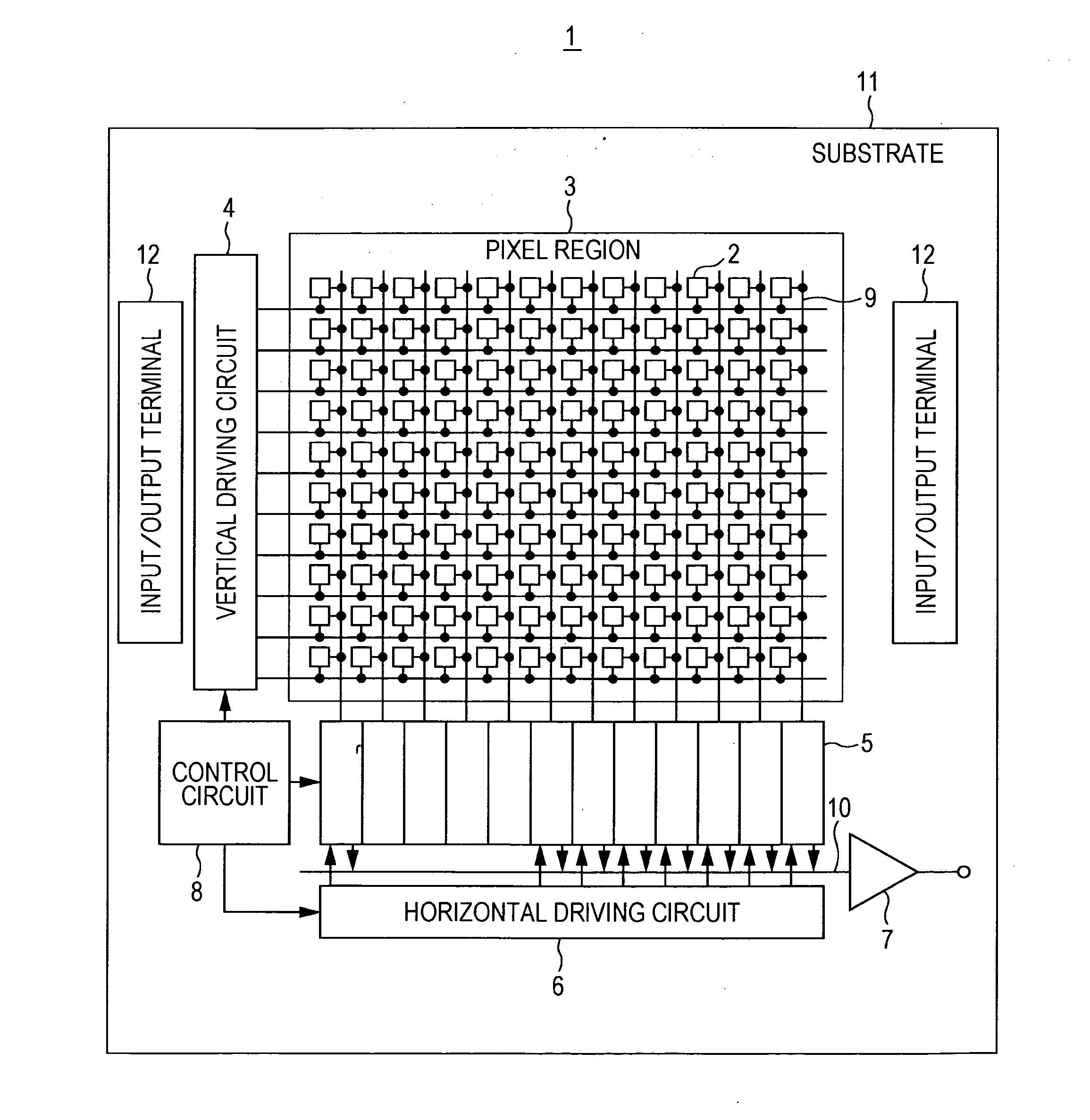
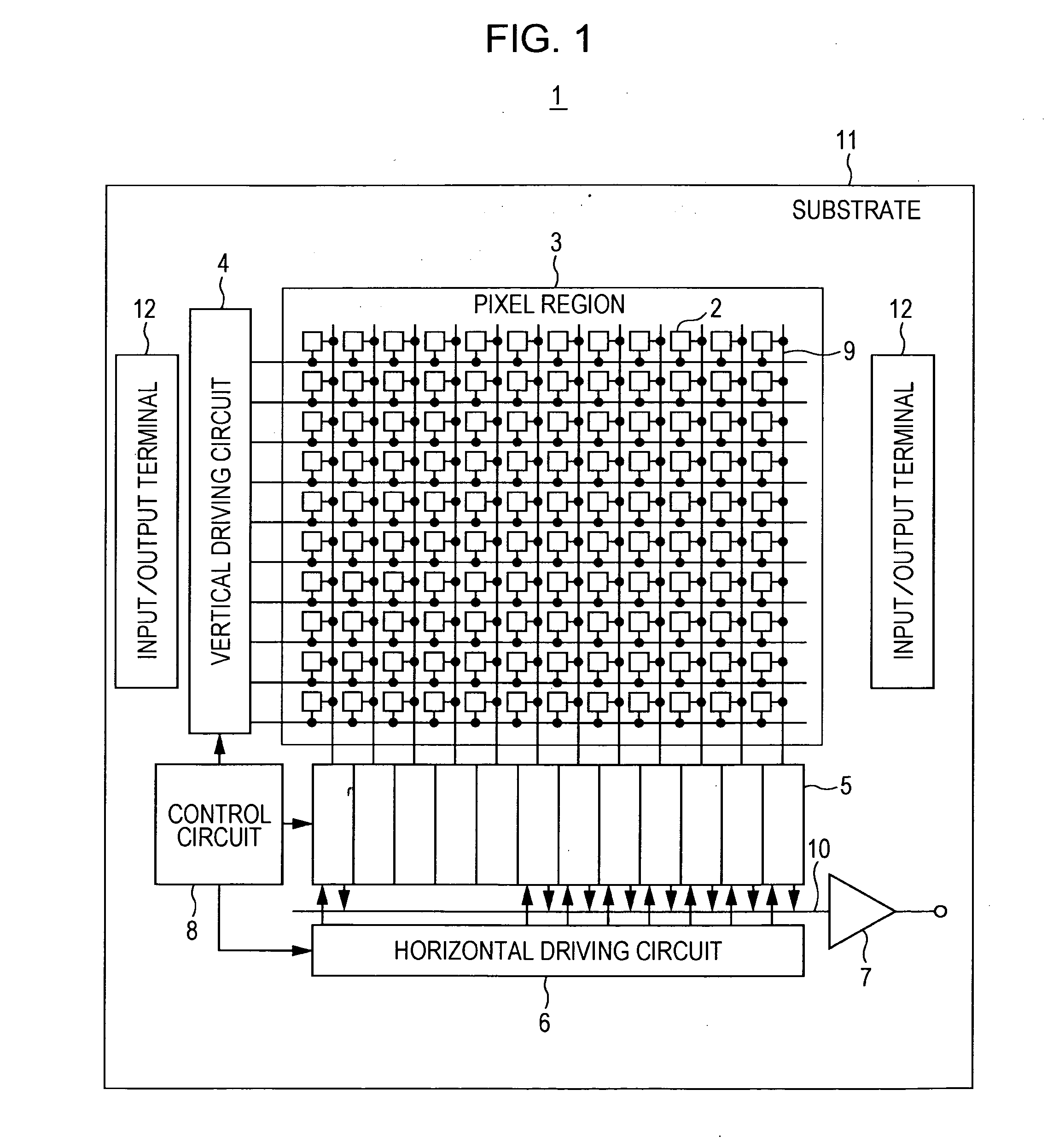
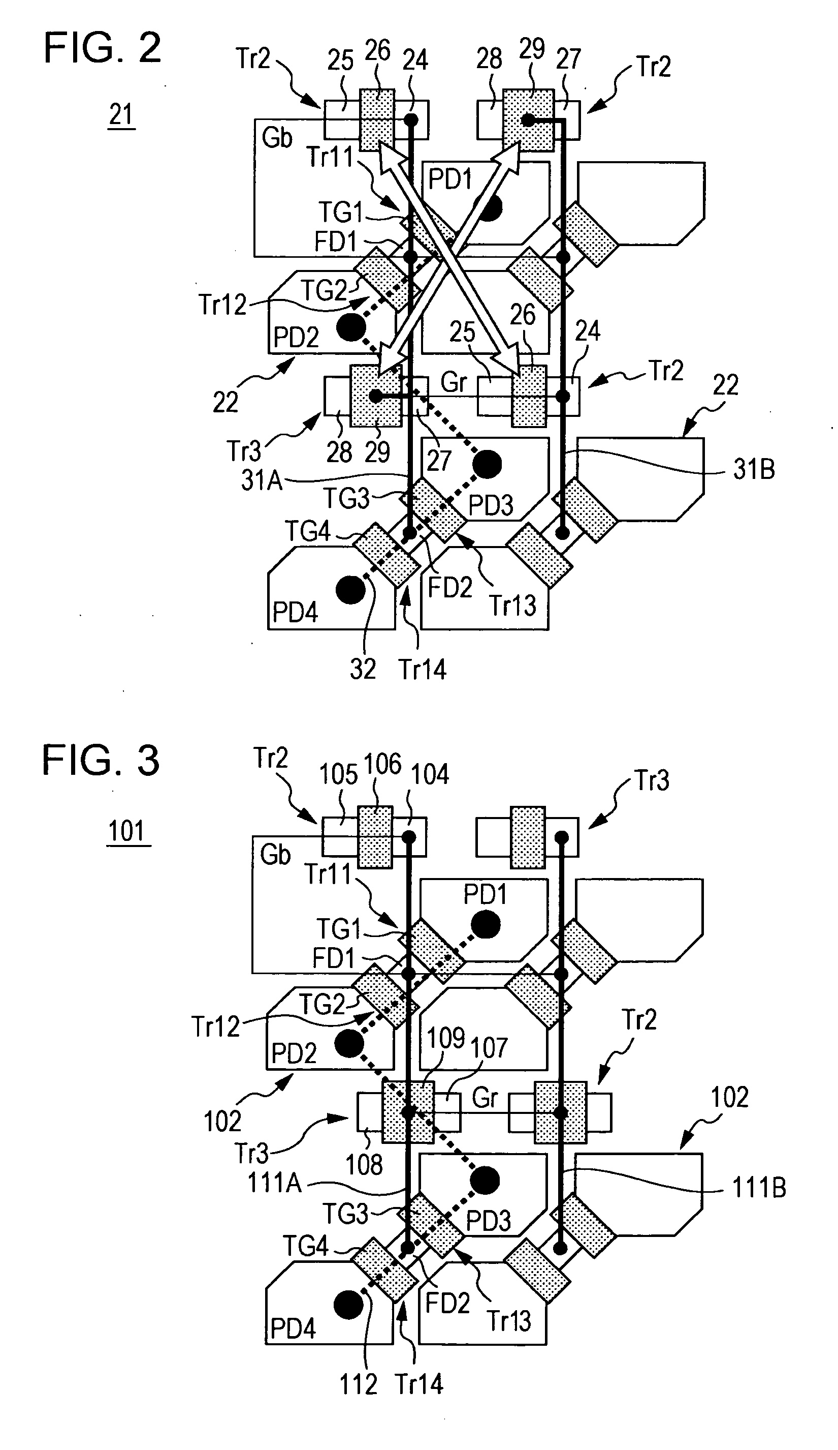
[0089]FIG. 2 shows a solid-state imaging device, that is, a CMOS solid-state imaging device according to a first embodiment of the present invention. FIG. 2 shows the schematic configuration of main portions applied to the CMOS solid-state imaging device in which pixel transistors of the 3-transistor type are provided and a plurality of shared pixels having a zigzag 4-pixel shared structure is arranged. The present embodiment is characterized in the arrangement of the pixel transistors and will be described in comparison with a Comparative Example 1 of FIG. 3.

[0090]FIG. 22 shows an equivalent circuit of the shared pixels having the 4-pixel shared structure of the 3-transistor type. The shared pixels according to the present example include four photodiodes PD [PD1 to PD4] which are the photoelectric conversion portions, four transfer transistors Tr1 [Tr11 to Tr14], one reset transistor Tr2, and one amplification t...

second embodiment

4. Second Embodiment

Configuration Example of Solid-state Imaging Device

[0104]FIG. 4 shows a solid-state imaging device, that is, a CMOS solid-state imaging device according to a second embodiment of the present invention. FIG. 4 shows the schematic configuration of main portions applied to the CMOS solid-state imaging device in which pixel transistors of the 4-transistor type are provided and a plurality of shared pixels having a zigzag 4-pixel shared structure is arranged. The arrangement of the pixel transistors and the like of the present embodiment will be described in comparison with Comparative Example 2 of FIG. 5.

[0105]FIG. 23 shows an equivalent circuit of the shared pixels having the 4-pixel shared structure of the 4-transistor type. The shared pixels according to the present example include four photodiodes PD [PD1 to PD4] which are the photoelectric conversion portions, four transfer transistors Tr1 [Tr11 to Tr14], one reset transistor Tr2, one amplification transistor Tr...

third embodiment

5. Third Embodiment

Configuration Example of Solid-State Imaging Device

[0113]FIG. 6 shows a solid-state imaging device, that is, a CMOS solid-state imaging device according to a third embodiment of the present invention. FIG. 6 shows the schematic configuration of main portions applied to the CMOS solid-state imaging device in which pixel transistors of the 4-transistor type are provided and a plurality of shared pixels having a zigzag 4-pixel shared structure is arranged. The arrangement of the pixel transistors and the like of the present embodiment will be described in comparison with a Comparative Example 3 of FIG. 7.

[0114]First, the solid-state imaging device according to Comparative Example 3 of FIG. 7 will be described. The solid-state imaging device 124 of Comparative Example 3 is a CMOS solid-state imaging device having a zigzag 4-pixel shared structure using color filters of the Bayer array.

[0115]Since the other configuration is the same as that of the above-described Compa...


PUM


Abstract

A solid-state imaging device includes a pixel region in which shared pixels which share pixel transistors in a plurality of photoelectric conversion portions are two-dimensionally arranged. The shared pixel transistors are divisionally arranged in a column direction of the shared pixels, the pixel transistors shared between neighboring shared pixels are arranged so as to be horizontally reversed or/and vertically crossed, and connection wirings connected to a floating diffusion portion, a source of a reset transistor and a gate of an amplification transistor in the shared pixels are arranged along the column direction.

Description

BACKGROUND OF THE INVENTION[0001]1. Field of the Invention[0002]The present invention relates to a CMOS type solid-state imaging device and an electronic apparatus including the solid-state imaging device, which is applicable to, for example, a camera or the like.[0003]2. Description of the Related Art[0004]As a solid-state imaging device, a CMOS solid-state imaging device is known. Since the CMOS solid-state imaging device has a low power supply voltage and low power consumption, the CMOS solid-state imaging device is used in digital still cameras, digital video cameras, various mobile terminals such as a mobile phone including a camera therein, printers, and the like.[0005]In the CMOS solid-state imaging device, a pixel arranged in a pixel region includes a plurality of pixel transistors in addition to photodiodes PD which are photoelectric conversion portions, unlike a CCD solid-state imaging device. In a general unit pixel, the pixel transistor includes four transistors, namely,...

Claims


Application Information

Patent Timeline
IPC IPC(8): H04N5/228H04N5/335
CPCH01L27/14603H01L27/14641H01L27/148H01L27/14643H04N5/3745H01L27/14612H01L27/1461H01L27/14636H01L27/14614H01L27/14625H04N25/77H04N25/767H04N25/745H04N25/75
Inventor KIDO, HIDEOYAMAMOTO, ATSUHIKOYAMADA, AKIHIRO
Owner SONY CORP
Why Eureka
Try Eureka