Stacked Integracted Circuit Verification

Inactive Publication Date: 2011-07-28
HOGAN WILLIAM MATTHEW +2
View PDF2 Cites 22 Cited by
  • Summary
  • Abstract
  • Description
  • Claims
  • Application Information

AI Technical Summary

Benefits of technology

[0015]Aspects of the invention relate to techniques of more performing physical verification processes for stacked integrated circuit devices. According to various implementations of the invention, for a stacked integrated circuit device, an interface between a first two-dimensional integrated circuit device and a second two-dimensional integrated circuit device is identified. More particularly, one or more layers on a first two-dimensional integrated circuit device are identified. The one or more layers on the second two-dimensional integrated circuit device that will be electrically connected with the one or more layers on the first two-dimensional integrated circuit device are identified as well. The design data for the identified layers in the first and second two-dimensional integrated circuit devices are then combined and physically verified as a single set of interface design data. The design data for the first two-dimensional integrated circuit device and the second two-dimensional integrated circuit device are then separately physically verified. Once the interface design data

Problems solved by technology

Moreover, the sizes of the polygons are limited physically by the maximum beam aperture size available to the tool.
As is has become more and more difficult to reduce transistor size further, however, some designers have begun stacking integrated circuit elements on top of one another in a third dimension to increase the functionality of integrated circuit devices without increasing the size of their footprints.
Doing so, however, over complicates the verification process of TSV designs.
It also creates additional disruption to existing veri

Method used


Image

  • Stacked Integracted Circuit Verification
  • Stacked Integracted Circuit Verification
  • Stacked Integracted Circuit Verification

Examples


Embodiment Construction

Exemplary Operating Environment

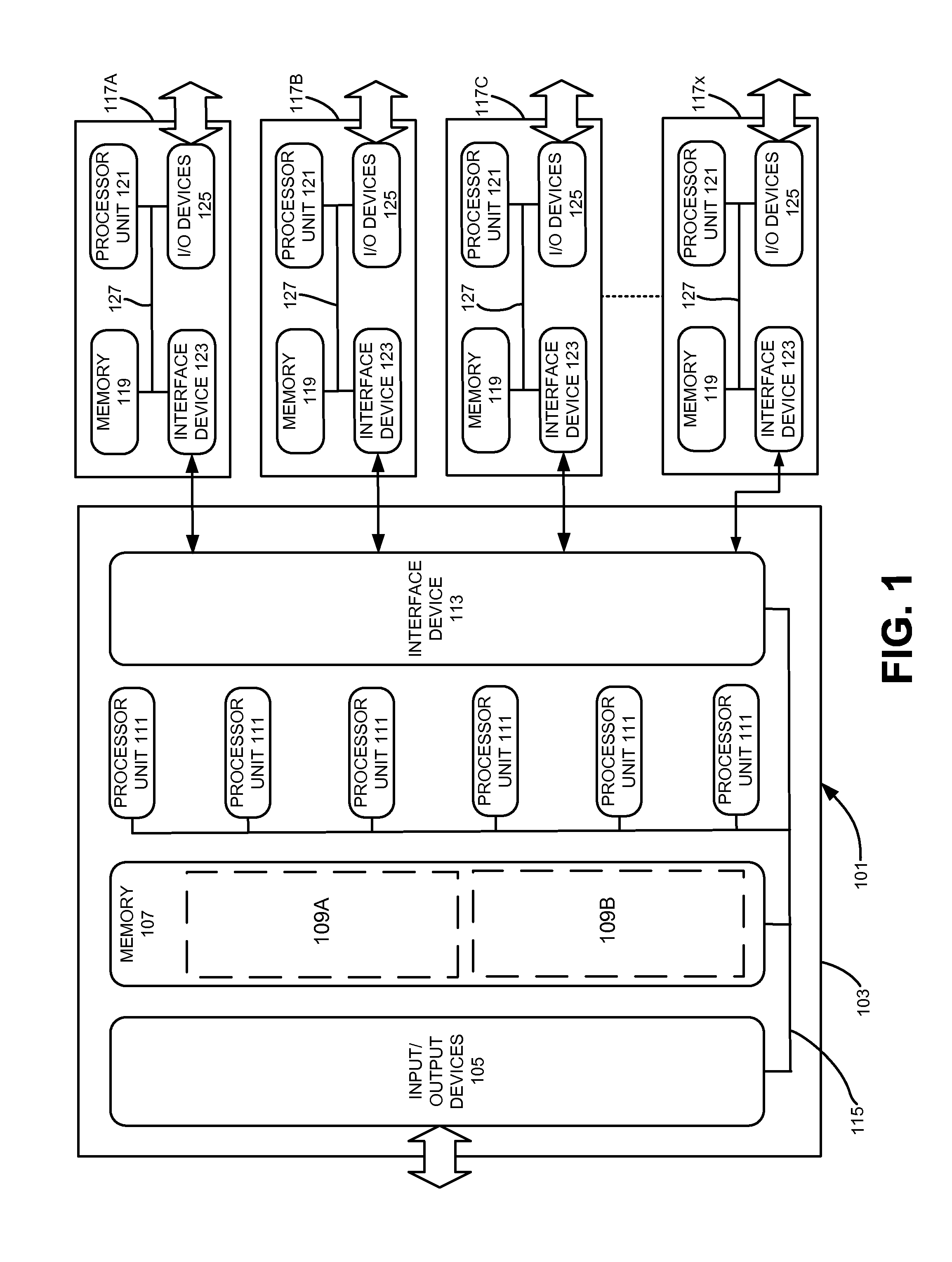
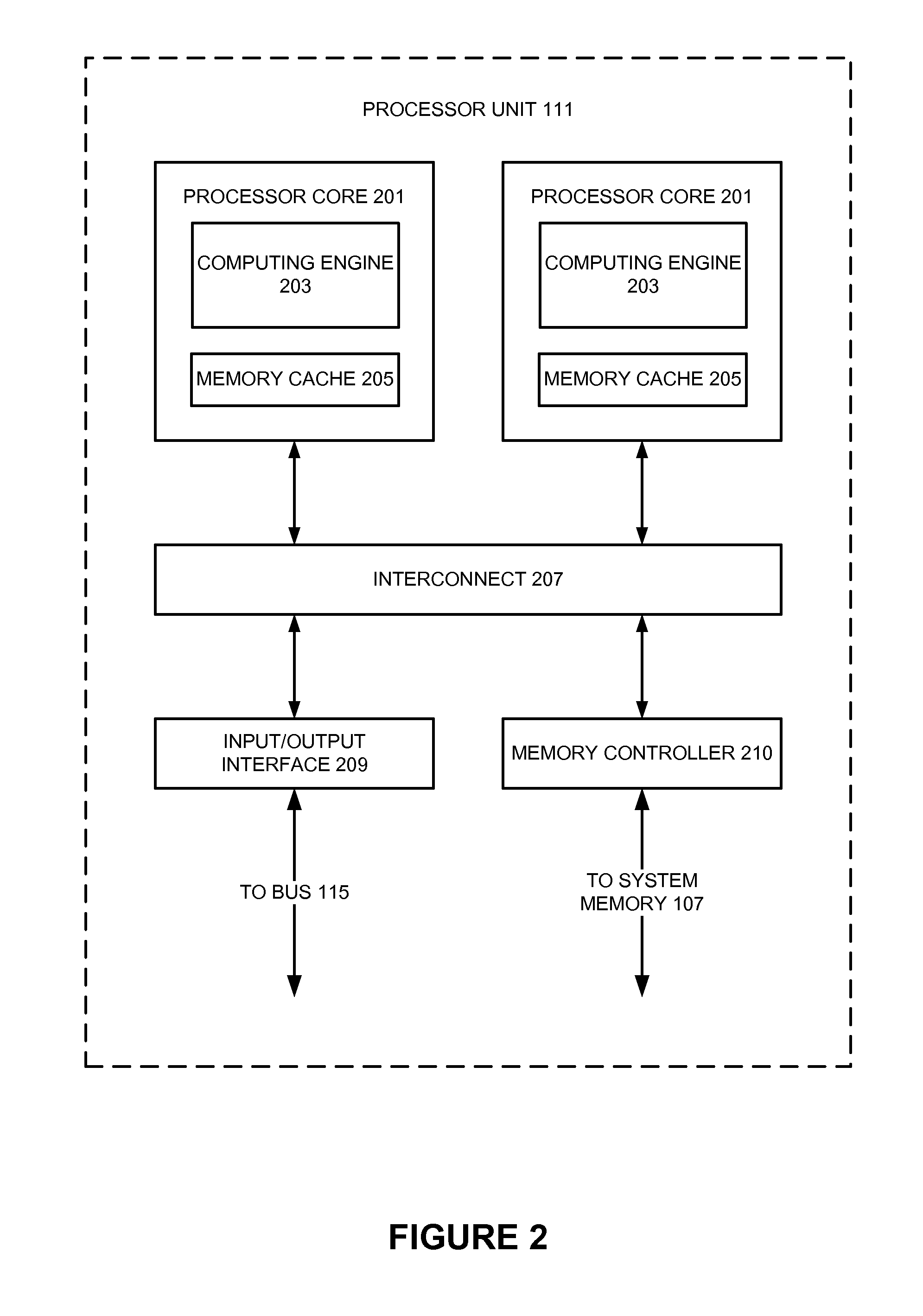
[0022]The execution of various electronic design automation processes according to embodiments of the invention may be implemented using computer-executable software instructions executed by one or more programmable computing devices. Because these embodiments of the invention may be implemented using software instructions, the components and operation of a generic programmable computer system on which various embodiments of the invention may be employed will first be described. Further, because of the complexity of some electronic design automation processes and the large size of many circuit designs, various electronic design automation tools are configured to operate on a computing system capable of simultaneously running multiple processing threads. The components and operation of a computer network having a host or master computer and one or more remote or servant computers therefore will be described with reference to FIG. 1. This operating envir...


PUM


Abstract

Techniques for performing physical verification processes for stacked integrated circuit devices. An interface between a first two-dimensional integrated circuit device and a second two-dimensional integrated circuit device is identified. The design data for the identified layers in the first and second two-dimensional integrated circuit devices are then combined and physically verified as a single set of interface design data. The design data for the first two-dimensional integrated circuit device and the second two-dimensional integrated circuit device are then separately physically verified. Once the interface design data, the first two-dimensional integrated circuit device design data and the second two-dimensional integrated circuit device design data have been physically verified, the verified design can be recombined to form verified design data corresponding to a stacked integrated circuit device.

Description

RELATED APPLICATIONS[0001]This application claims priority to U.S. Provisional Patent Application No. 61 / 235,871 entitled “Stacked Integrated Circuit Verification,” filed on Aug. 21, 2009, and naming William M. Hogan and Dusan Petranovi as inventors, which application is incorporated entirely herein by reference.FIELD OF THE INVENTION[0002]The present invention is directed to the verification of stacked integrated circuit devices. Various implementations of the invention may be useful for verifying a design for creating a single circuit device by stacking and electrically connecting multiple integrated circuit devices.BACKGROUND OF THE INVENTION[0003]Electronic circuits, such as integrated microcircuits, are used in a variety of products, from automobiles to microwaves to personal computers. Designing and fabricating microcircuit devices typically involves many steps, known as a “design flow.” The particular steps of a design flow often are dependent upon the type of microcircuit be...

Claims


Application Information

Patent Timeline
IPC IPC(8): G06F17/50
CPCG06F17/5081G06F30/398
Inventor HOGAN, WILLIAM MATTHEWPETRANOVIC, DUSANASLYAN, ARA
Owner HOGAN WILLIAM MATTHEW
Why Eureka
Try Eureka