Display device and manufacturing method thereof

a technology of a display device and a manufacturing method, which is applied in the manufacture of electrode systems, electric discharge tubes/lamps, instruments, etc., can solve the problems of deformation of the surface of the panel-like member, deformation of the display quality,

Active Publication Date: 2011-08-04
PANASONIC LIQUID CRYSTAL DISPLAY CO LTD +1
View PDF5 Cites 48 Cited by
  • Summary
  • Abstract
  • Description
  • Claims
  • Application Information

AI Technical Summary

Benefits of technology

[0111]Several examples for the method of manufacturing a liquid crystal display device according to the invention are to be described. In the following examples, only the step o

Problems solved by technology

If such foams develop in the display area, the display quality is degraded by the foams.
Further, when the panel-like member is bonded to the liquid crystal display panel, the surface of the pa

Method used


Image

  • Display device and manufacturing method thereof
  • Display device and manufacturing method thereof
  • Display device and manufacturing method thereof

Examples


example 1

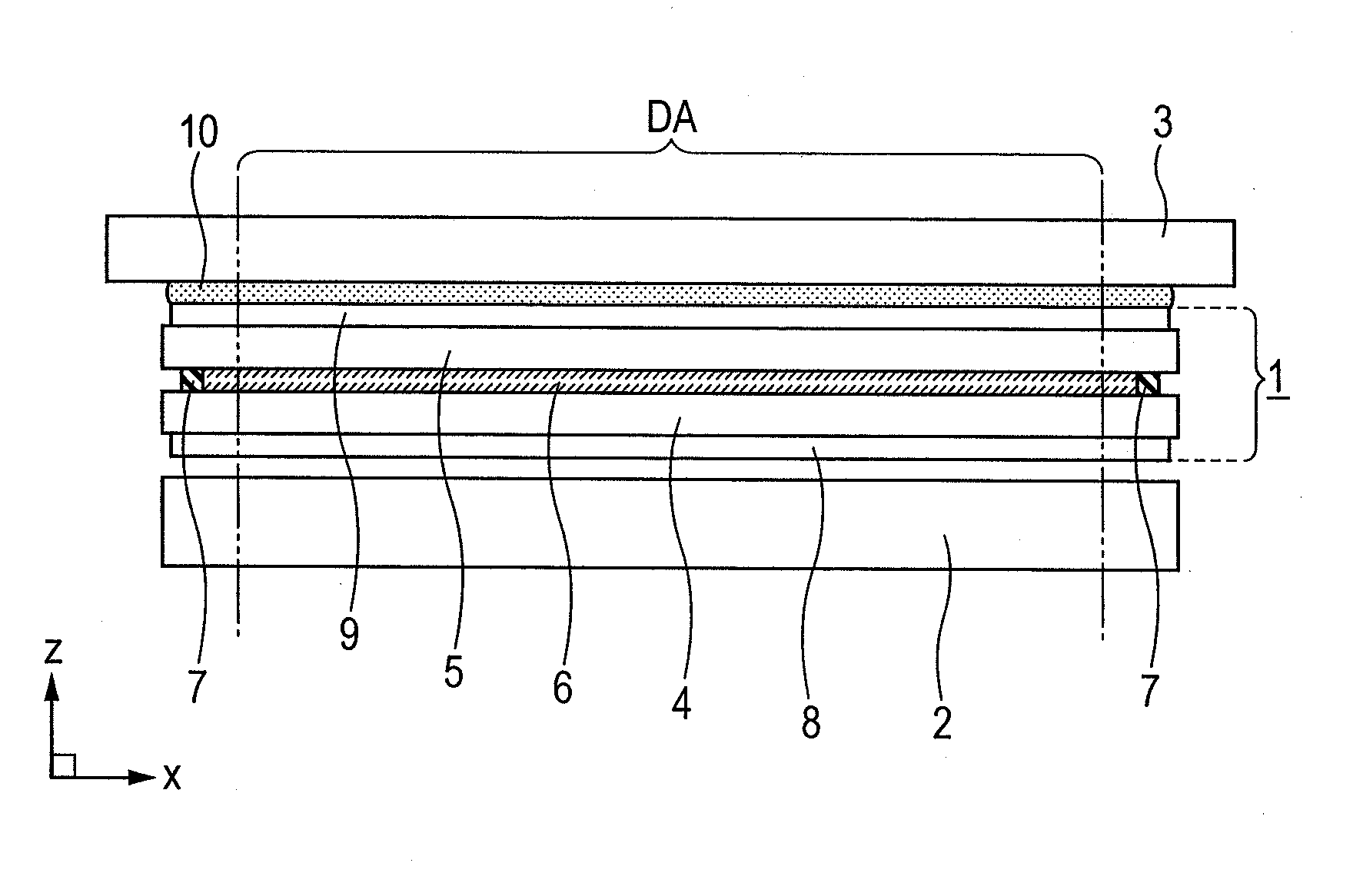
[0112]FIGS. 9 and 10 are schematic views of assistance for explaining main steps in the method of manufacturing the liquid crystal display device of Example 1 according to the invention.

[0113]FIG. 9 is a schematic cross sectional view showing a first stage in the step of curing an ultraviolet curable resin. FIG. 10 is a schematic cross sectional view showing a second stage in the step of curing the ultraviolet curable resin.

[0114]In the method of manufacturing the liquid crystal display device in Example 1, the first adhesive portion 10a of the adhesive 10 is adapted to have a different bonding strength from the second adhesive portion 10b of the adhesive 10 by changing the irradiation condition of ultraviolet rays when the panel-like member 3 is bonded to the liquid crystal display panel 1 by using an ultraviolet curable resin.

[0115]When a radical reaction type ultraviolet curable resin is as the adhesive 10 for example, the radical reaction (curing reaction) proceeds more and the ...

example 2

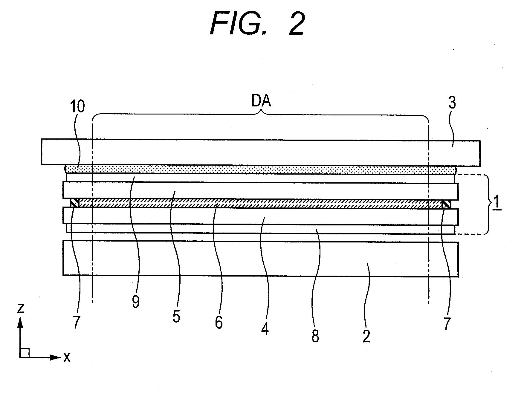
[0123]FIGS. 11 to 15 are schematic views of assistance for explaining main steps in the method of manufacturing the liquid crystal display device of Example 2 according to the invention.

[0124]FIG. 11 is a schematic perspective view showing a first stage in the step of coating an uncured ultraviolet curable resin. FIG. 12 is a schematic plan view showing a second stage in the step of coating the uncured ultraviolet curable resin. FIG. 13 is a schematic cross sectional view showing an example for the cross sectional configuration at the position along line B-B′ in FIG. 12. FIG. 14 is a schematic cross sectional view showing an example of a stage in the course of the step of closely bonding the panel-like member to the liquid crystal display panel. FIG. 15 is a schematic cross sectional view showing the state in which the panel-like member is closely bonded to the liquid crystal display panel.

[0125]The method of manufacturing the liquid crystal display device of Example 1 is basically ...


PUM

PropertyMeasurementUnit
Compositionaaaaaaaaaa
Viscosityaaaaaaaaaa
Strengthaaaaaaaaaa

Abstract

Disclosed is a display device in which reliable bonding strength and high reparability are compatible when a panel-like member is bonded to a display panel.
The display device comprises: a display panel; and a panel-like member bonded to the display panel with an adhesive made of an ultraviolet curable resin; wherein the adhesive includes a first adhesive portion and a second adhesive portion, the first adhesive portion being provided outside of a display area of the display panel and formed in a circular shape to surround the display area, the second adhesive portion prevailing in an area surrounded by the first adhesive portion, the first adhesive portion being different in a modulus of elasticity from the second adhesive portion, and wherein the modulus of elasticity of the second adhesive portion is smaller than the modulus of elasticity of the first adhesive portion.

Description

CLAIM OF PRIORITY[0001]The present application claims priority from Japanese Patent Application JP 2010-022709 filed on Feb. 4, 2010, the content of which is hereby incorporated by reference into this application.BACKGROUND OF THE INVENTION[0002]1. Field of the Invention[0003]The present invention relates to a display device and a manufacturing method thereof. The invention particularly relates to a technique which is effective when applied to a liquid crystal display device in which a panel-like member such as a protective panel is bonded to a liquid crystal display panel.[0004]2. Description of the Related Art[0005]Liquid crystal display devices have been used so far, for example, as displays (display devices) for mobile electronic devices such as mobile phone terminals or digital cameras.[0006]In recent years, size and weight of mobile electronic devices have been decreased more and more. Along with this, the thickness of liquid crystal display devices has also been decreased. Th...

Claims


Application Information

Patent Timeline
IPC IPC(8): G02F1/1333H01J9/20
CPCH01J9/20G02F1/1333G02F1/1309G02F1/133308G02F2202/023G02F2202/28G02F1/133331
Inventor KOBAYASHI, SETSUOISHII, AKIRAKATSUYAMA, MASANORITANABE, SHINJISENTO, KIYOSHI
Owner PANASONIC LIQUID CRYSTAL DISPLAY CO LTD
Why Eureka
Try Eureka