Composite magnetic material and electromagnetic interference suppressor member using the same

a technology of electromagnetic interference and suppressor member, applied in the field of composite magnetic materials, can solve the problems of inductive noise, frequency noise, and mainly caused by high frequency noise of active elements

Inactive Publication Date: 2005-12-06
TOKIN CORP
View PDF6 Cites 35 Cited by
  • Summary
  • Abstract
  • Description
  • Claims
  • Application Information

AI Technical Summary

Benefits of technology

[0019]It is another object of the present invention to provide a composite magnetic material capable of meeting a requirement of severe vibration resistance, shock resistance, and adaptability for a complex shape.
[0020]It is still another object of the present invention to provide a composite magnetic material which is excellent in flexibility, stickable to, for example, a FPC, an FFC, or a curved surface of a casing of an electronic equipment and further excellent in fire resistance.
[0023]It is a still further object of the present invention to provide an electronic device which has a compact size and a light weight and can inhibit effectively an electromagnetic interference by provision of the electromagnetic interference suppressing body.
[0024]It is a yet further object of the present invention to provide a printed circuit board which has a sufficient shield effect against the transmission of electromagnetic wave without deteriorating a shield effect of the printed circuit board with an electromagnetic shield, and does not promote at least a magnetic coupling due to a reflection of an electromagnetic wave.

Problems solved by technology

In such a logic circuit or the like, high-speed signals are accompanied by sudden variation of voltage and current, so that the active elements generate inductive noise which is high frequency noise.
The high frequency noise is mainly caused by the inductive noise generated by the active element.
Since printed wires between the electronic devices mounted with high mounting density or wires between modules are placed near to each other, and since the signal processing speed is increased as described above, the induced high frequency magnetic field increases the electromagnetic coupling between wires on the printed circuit board due to radiation noise.
The radiation noise as generated is radiated through an external connection terminal outside the device to cause a harmful influence upon the other devices.
The harmful influence to the other devices and the malfunction of the electronic apparatus are collectively called as an electromagnetic obstacle.
In a printed circuit board or others on which electronic parts including active elements are mounted in a high density, those known countermeasure against the electromagnetic obstacle (noise suppression) has disadvantages, for example, that special knowledge and experience are required therefor and a long time is required for establishment of the countermeasure.
Particularly, the use of the filter as mentioned above has disadvantages that the filter used for removing noises is too expensive, that a space mounting the filter is often limited, that a work of mounting a filter is accompanied with a difficulty, and that many steps are required for assembling a device including the filter or the like to result in high cost.
In addition, suppression against an electromagnetic induction and interference by undesired electromagnetic wave which are generated between devices placed in the same circuit is not sufficient in the prior art.
Furthermore, for miniaturization of and lightening the electronic device, the method of removing a problem from circuit is disadvantageous and it is required to remove a filter and a mounting space thereof.

Method used


Image

  • Composite magnetic material and electromagnetic interference suppressor member using the same
  • Composite magnetic material and electromagnetic interference suppressor member using the same
  • Composite magnetic material and electromagnetic interference suppressor member using the same

Examples


first example

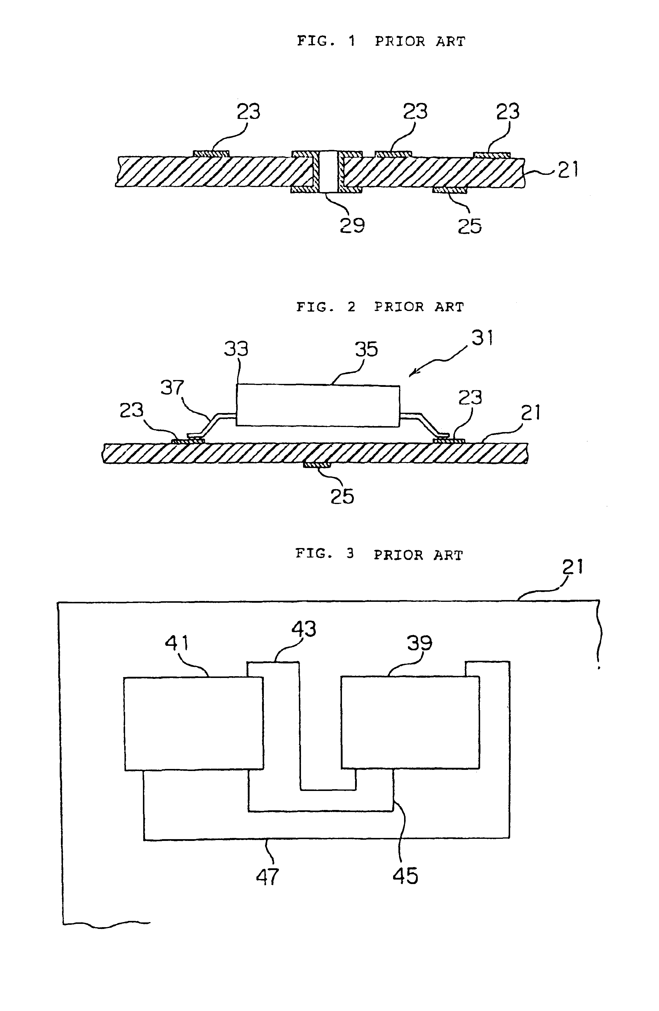
[0138]Referring to FIG. 14, a printed circuit board 21 a is applied with the electromagnetic interference suppressing body using the composite magnetic material of the present invention. The printed circuit board are provided with the conductive circuit patterns 23, 25, and 29 and others thereon, which are omitted in the figure, in the similar manner as the conventional printed circuit board shown in FIG. 1.

[0139]The printed circuit board 21a of a first example, itself, has a different structure from the conventional one. That is, the first example of the printed circuit board 21a has a conductive support plate or a conductive soft magnetic support layer 75. The printed circuit board 21a, further, has a pair of composite magnetic layers 77a on both sides of the conductive support layer 75. The composite magnetic layer 77a comprises soft magnetic powder particles 79 and an organic binder 81. The composite magnetic layer 77 have a plurality of anisotropic magnetic fields and a plurali...

second example

[0140]Referring to FIG. 15, a second example of the printed circuit board comprises a conductive support layer 75 and composite magnetic layers 77b formed on both sides of the conductive support layer 75. The printed circuit board 21b further has a pair of dielectric layers 83 on both sides of the composite magnetic layers 77b in a different structure from that shown in FIG. 14. Accordingly, the second example of the printed circuit board has a structure wherein composite magnetic layers 77b are interposed between the conductive support layer 75 and each of dielectric layer 83. The composite magnetic layer 77b is similar to the first example and have a plurality of anisotropic magnetic fields and a plurality of magnetic resonances in the magnetic less term. Furthermore, the composite magnetic layer 77b also contains an organic binder 81 forming its matrix. Each of the dielectric layers 83 comprises a dielectric powder 85 and an organic binder 81. The organic binder 81 is contained f...

third example

[0141]Referring to FIG. 16, a third example of the printed circuit board comprises a conductive support layer 75 and composite magnetic layers 77c formed on both sides of the conductive support layer 75 (which is a similar reference number to the conductive support plate). Each of the composite magnetic layers 77c contains a soft magnetic powder 79, a dielectric powder 85 and an organic binder 81. The composite magnetic layer 77c has a different anisotropic magnetic fields in a similar manner to the first and second examples.

[0142]In the first to the third examples as mentioned above, the conductive support plate or conductive soft magnetic support layer 75 may be, for example, a conductive plate, a conductive mesh plate, or a woven fabric of conductive fibers, a metal plate such as a copper thin plate, stainless steel thin plate, aluminum thin plate and others, or a so called punched metal plate having fine holes formed in them, an expanded metal plate formed by fine-slitting a thi...


PUM

PropertyMeasurementUnit
specific surface areaaaaaaaaaaa
lengthaaaaaaaaaa
thicknessaaaaaaaaaa

Abstract

A composite magnetic material is provided for use as an electromagnetic interference suppressing body for effectively suppressing an electromagnetic interference within a high frequency apparatus including a mobile communication terminal. The composite magnetic material consists essentially of a soft magnetic powder and an organic binder and is electrically non-conductive and has at least two magnetic resonances caused by at least two anisotropic magnetic fields (Hk). In the composite magnetic material, the anisotropic magnetic fields (Hk) are different in strength from each other.

Description

[0001]This application is a continuation-in-part of Ser. No. 09 / 459,431, filed Dec. 3, 1999, now abandoned, which is a continuation-in-part of both Ser. No. 09 / 374,860 filed Aug. 16, 1999 now abandoned, which is a continuation-in-part of Ser. No. 09 / 066,382, filed Apr. 29, 1998, which is the U.S. national phase of PCT / JP97 / 03067, filed Sep. 2, 1997 and a continuation of Ser. No. 08 / 809,220, filed May 12, 1997 now abandoned, which is the U.S. national phase of PCT / JP96 / 02040, filed Jul. 22, 1996.BACKGROUND OF THE INVENTION[0002](1) Field of the Invention[0003]The present invention relates to composite magnetic materials comprising soft magnetic powders kneaded with and dispersed in an organic binder and, in particular, to the composite magnetic material excellent in a characteristic of complex magnetic permeability effective in suppressing an electromagnetic interference which is a problem in high frequency electronic circuits / devices, and to a method for producing the same.[0004]The...

Claims


Application Information

Patent Timeline
Patent Type & Authority Patents(United States)
IPC IPC(8): H01F1/22H01L23/552H05K1/02H05K1/03H05K9/00
CPCH01F1/22H01L23/552H05K1/0233H05K9/0083H01L2924/3011H05K1/0373H01L2924/0002H01L2924/00
Inventor YOSHIDA, SHIGEYOSHISATO, MITSUHARUSUGAWARA, EISHUSHIMADA, YUTAKAONO, NORIHIKOITO, OSAMU
Owner TOKIN CORP
Why Eureka
Try Eureka