

TMR device with novel free layer structure
a free layer structure and tmr technology, applied in the field of high-performance tunneling magnetoresistive (tmr) sensor, can solve the problems of drastic drop in mr (tmr) ratio, inability to use cofeb/nife type free layer structure, and degraded tmr ratio, etc., to achieve the effect of improving the crystal orientation of layers
Active Publication Date: 2011-08-04
HEADWAY TECH INC
View PDF20 Cites 61 Cited by
- Summary
- Abstract
- Description
- Claims
- Application Information
AI Technical Summary
Benefits of technology
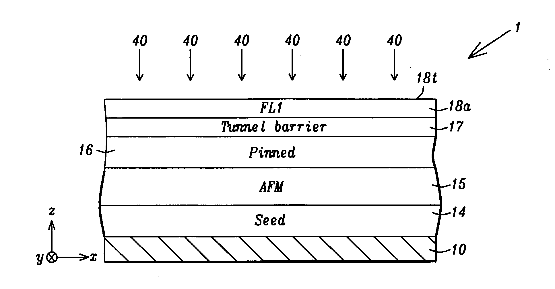
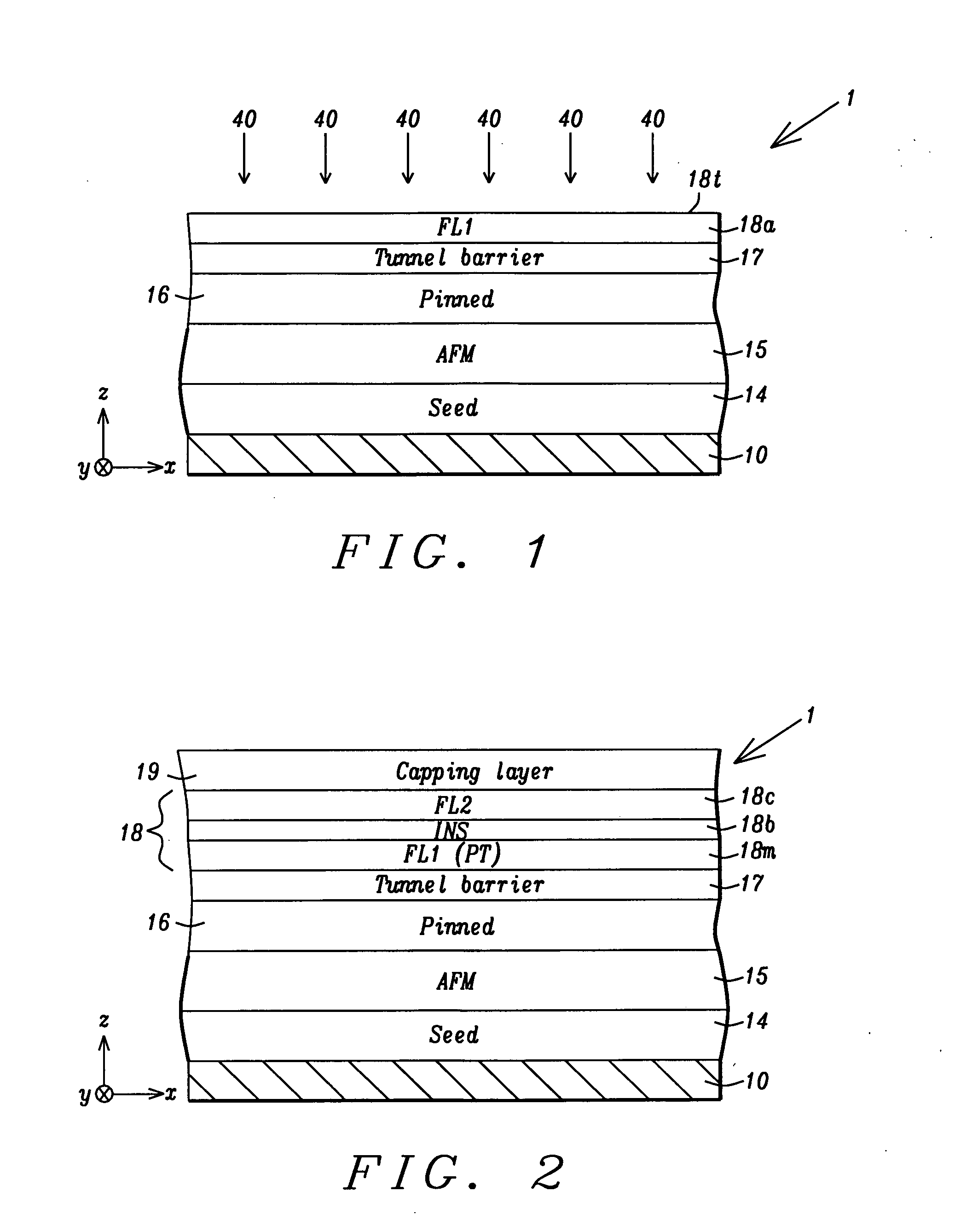
[0023]In yet another embodiment, the plasma treatment process may be applied to a top spin valve configuration represented by seed layer/FL2/INS/FL1(PT)/non-magnetic spacer/pinned/AFM/capping layer where the FL1 layer is treated with a weak plasm
Problems solved by technology
Unfortunately, the magnetostriction (λ) of a CoFeB free layer is considerably greater than the maximum acceptable value of about 5×10⁻⁶ for high density memory applications.
However, when using a CoF
Method used
View moreImage
Smart ImageViewing Examples

Examples
 PUM
| Property | Measurement | Unit |
|---|---|---|
| Temperature | aaaaa | aaaaa |
| Temperature | aaaaa | aaaaa |
| Lattice constant | aaaaa | aaaaa |
Abstract
A composite free layer having a FL1/insertion/FL2 configuration where a top surface of FL1 is treated with a weak plasma etch is disclosed for achieving enhanced dR/R while maintaining low RA, and low λ in TMR or GMR sensors. The weak plasma etch removes less than about 0.2 Angstroms of FL1 and is believed to modify surface structure and possibly increase surface energy. FL1 may be CoFe, CoFe/CoFeB, or alloys thereof with Ni, Ta, Mn, Ti, W, Zr, Hf, Tb, or Nb having a (+) λ value. FL2 may be CoFe, NiFe, or alloys thereof having a (−) λ value. The thin insertion layer includes at least one magnetic element such as Co, Fe, and Ni, and at least one non-magnetic element selected from Ta, Ti, W, Zr, Hf, Nb, Mo, V, Cr, or B. When CoFeBTa is selected as insertion layer, the CoFeB:Ta ratio is from 1:1 to 4:1.
Description
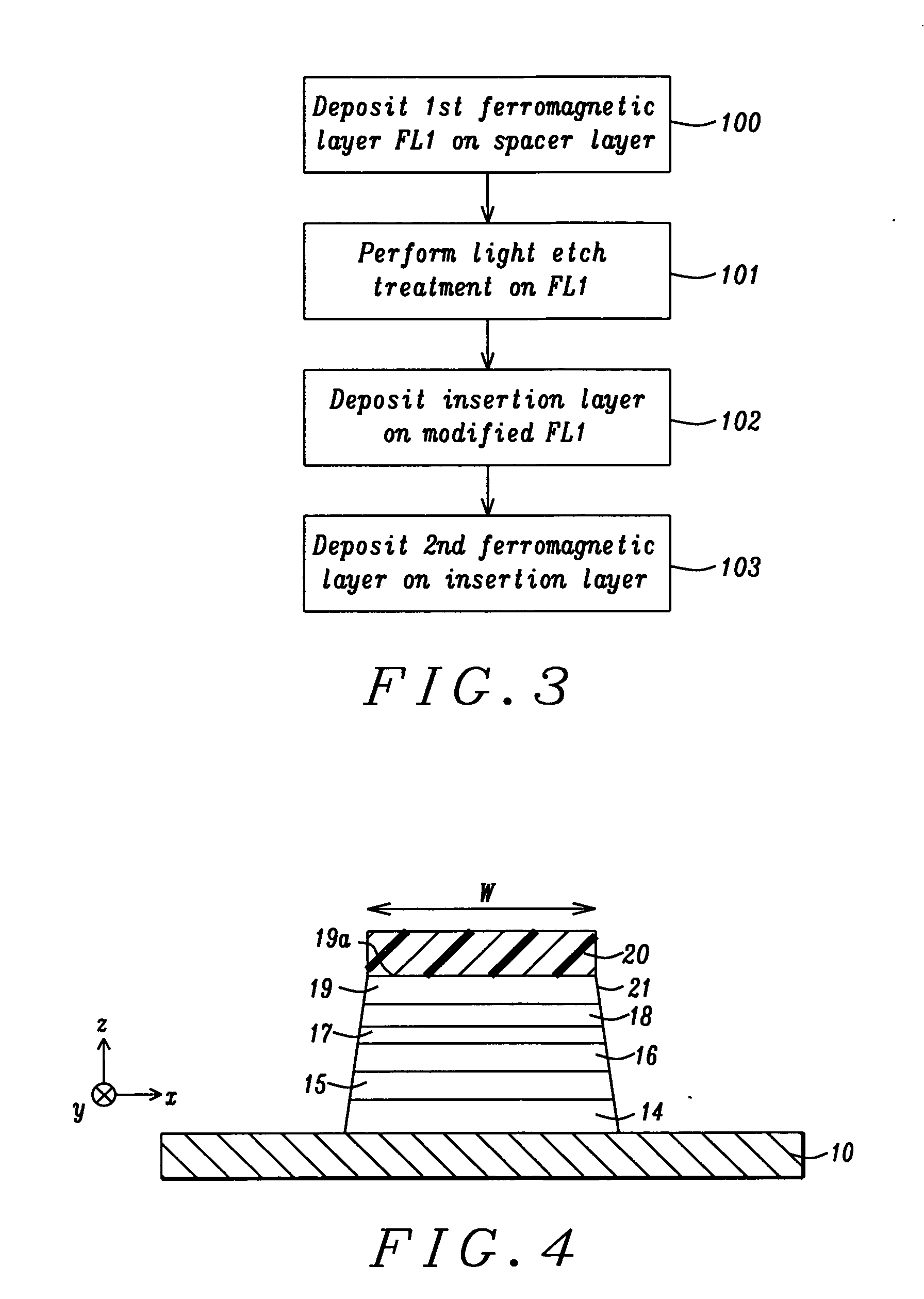
RELATED PATENT APPLICATIONS[0001]This application is related to the following: U.S. Patent Application Publication 2009 / 0122450; U.S. Patent Application Publication 2009 / 0121710; and Docket #HT08-035, Ser. No. 12 / 319,972; filing date Jan. 14, 2009; all assigned to a common assignee, and which are herein incorporated by reference in their entirety.FIELD OF THE INVENTION[0002]The invention relates to a high performance tunneling magnetoresistive (TMR) sensor in a read head and a method for making the same, and in particular, to a first ferromagnetic layer (FL1) in a composite free layer represented by a FL1 / INS / FL2 configuration in which the FL1 surface structure and surface energy are modified by a weak plasma etch treatment before an insertion layer (INS) and second ferromagnetic layer (FL2) are deposited thereby increasing the magnetoresistive (MR) ratio while maintaining strong coupling between the FL1 and FL2 magnetic layers.BACKGROUND OF THE INVENTION[0003]A TMR sensor otherwise...
Claims
Login to View More Application Information
Patent Timeline
 IPC IPC(8): G11B5/33B44C1/22
CPCB44C1/22Y10T29/49034Y10T29/49052G11B5/33G11B5/3906G11B2005/3996G11B5/3163H01F10/3254H01F10/3272H01F41/303G01R33/098G01R33/093H10N50/01H10N50/85H10N50/10G01R33/09
InventorZHAO, TONGWANG, HUI CHUANLI, MINZHANG, KUNLIANG
OwnerHEADWAY TECH INC