Semiconductor device and making method thereof

A manufacturing method and semiconductor technology, which is applied in semiconductor/solid-state device manufacturing, semiconductor devices, semiconductor/solid-state device components, etc., can solve the situation that the tungsten film is left behind after polishing, insufficiently polished, and cannot be accurately detected as an adherent layer and other problems to achieve the effect of preventing excessive polishing and insufficient polishing

Inactive Publication Date: 2005-06-08
PANASONIC CORP
View PDF1 Cites 0 Cited by
  • Summary
  • Abstract
  • Description
  • Claims
  • Application Information

AI Technical Summary

Problems solved by technology

[0003] When forming a tungsten insert, the problem that needs special attention is whether to correctly control the end point of the CMP process when removing the excess portion existing on the interlayer insulating film of the adhesion layer and the titanium film by the CMP method
[0004] When the end point of the CMP process for the tungsten film cannot be detected with high precision, the following problems will arise: that is, the contact resistance of the tungsten insert is significantly increased due to excessive polishing, or the adjacent tungsten is damaged due to insufficient polishing. Plugins are shorting each other
[0006] However, the above-mentioned conventional CMP method has the following problem: that is, since the time when the interlayer insulating film is exposed is regarded as the polishing end point, it is easy to cause excessive polishing.
[0008] However, the current problem is that it is impossible to accurately detect the end point of the CMP process on the tungsten film
exist Figure 8 In the case shown in (a), since the rotational torque increases sharply, it can be correctly detected that the polished film changes from a tungsten film to an adherent layer; Figure 8 In the case shown in (b), since the change in the rotational torque is small, it is impossible to accurately detect the change of the film to be polished from the tungsten film to the adhesion layer, that is, it is impossible to accurately detect the CMP process performed on the tungsten film. the end of
[0010] If the end point of the CMP process on the tungsten film cannot be accurately detected, the amount of polishing on the tungsten film will vary greatly, resulting in either remaining polishing of the tungsten film or forming a cut on the surface of the tungsten film.

Method used


Image

  • Semiconductor device and making method thereof
  • Semiconductor device and making method thereof
  • Semiconductor device and making method thereof

Examples


Embodiment 1

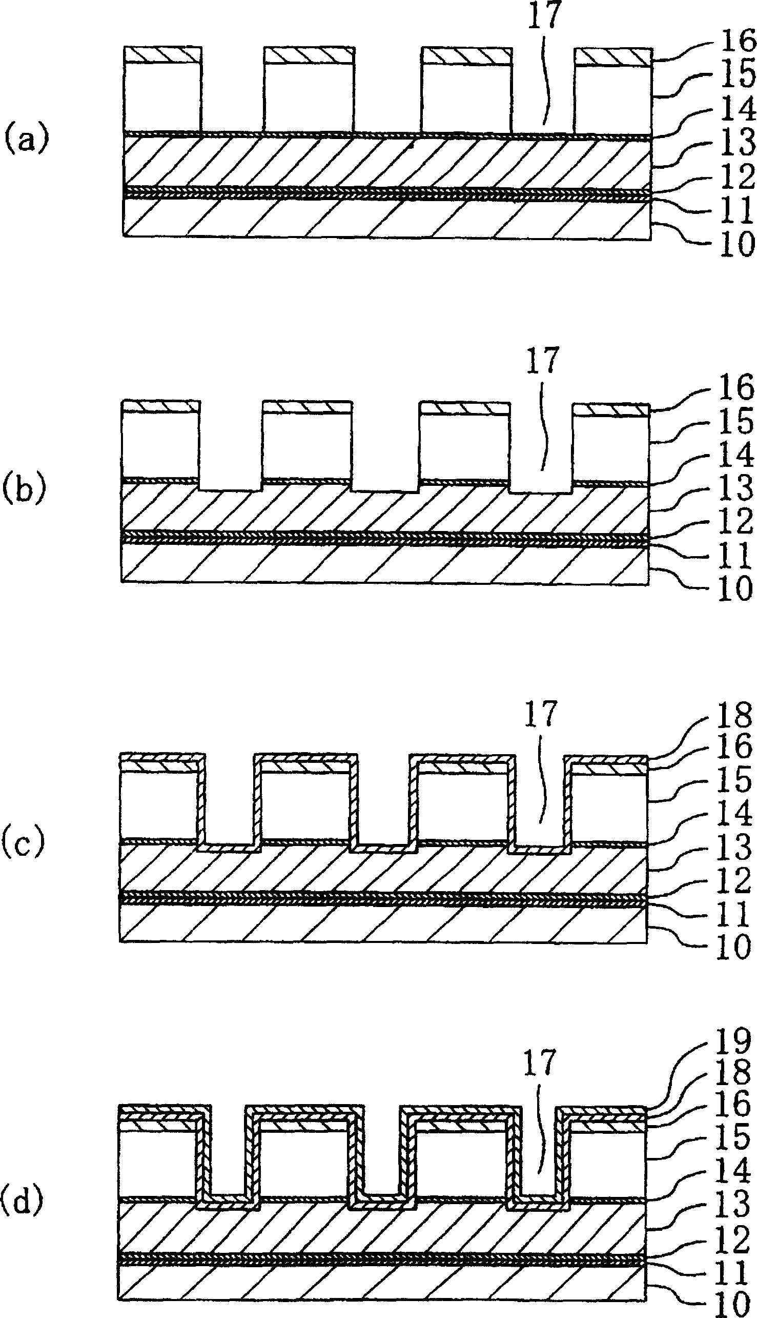
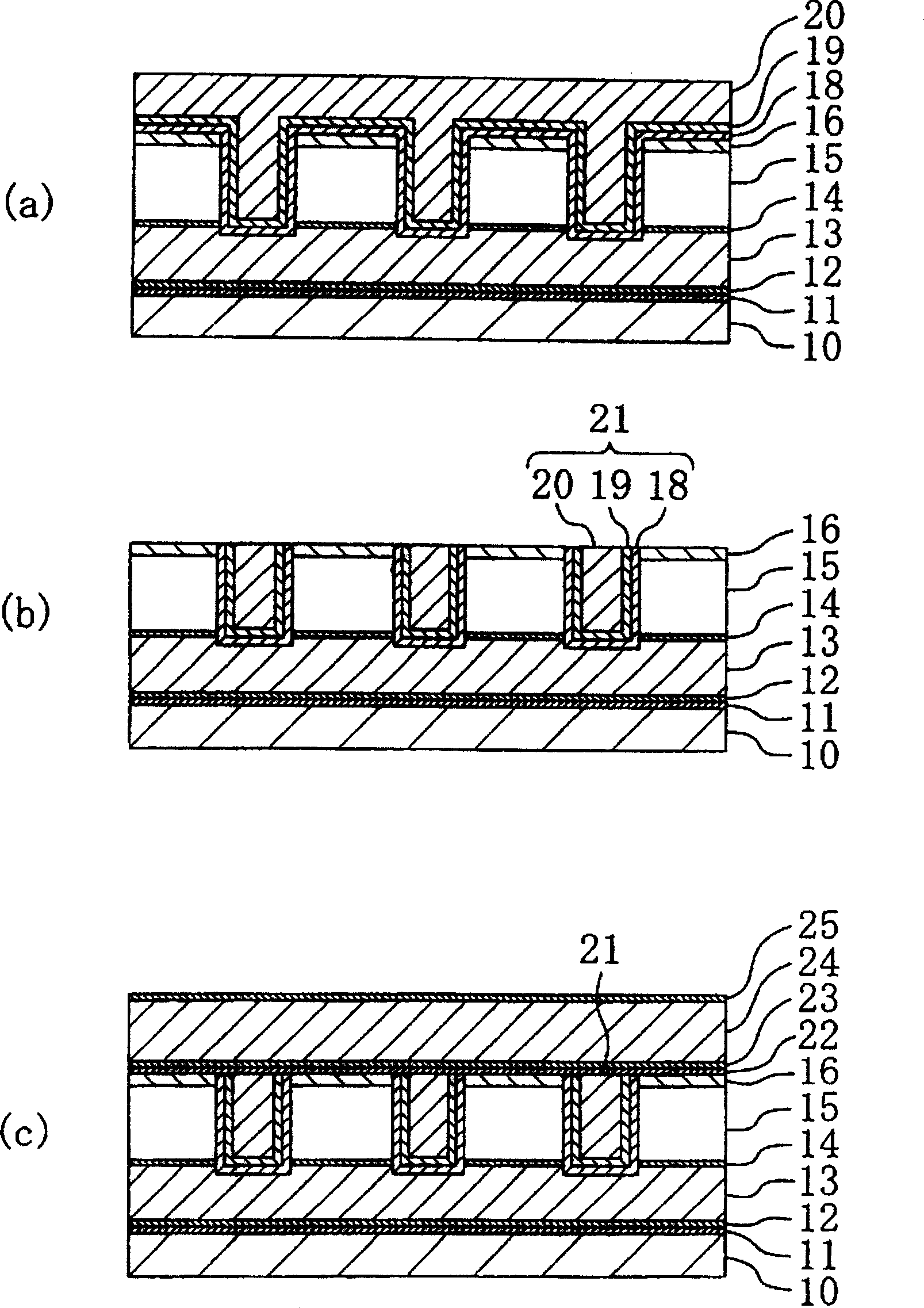
[0056] Below, refer to figure 1 (a)~(d) and figure 2 (a) to (c) The semiconductor device and its manufacturing method in Embodiment 1 of the present invention will be described.

[0057] First, if figure 1 As shown in (a), the lower layer metal wiring composed of the first titanium film 11, the first titanium nitride film 12, the first aluminum film 13 and the second titanium nitride film 14 is formed on the semiconductor substrate 10, and then A non-doped silicon oxide film (SiO 2 ) or an interlayer insulating film 15 made of a fluorine-doped silicon oxide film (SiOF).

[0058] Next, a silicon oxynitride film 16 as a hard film is formed on the interlayer insulating film 15 by plasma CVD, and then, the interlayer insulating film 15 is selectively etched using the silicon oxynitride film 16 as a mask. Etching is performed to form via holes 17 on the interlayer insulating film 15 . In addition, the first titanium film 11 and the first titanium nitride film 12 serve as an...

Embodiment 2

[0077] Below, refer to figure 1 (a)~(d) and figure 2 (a) to (c), the semiconductor device and the manufacturing method in Embodiment 2 of the present invention will be described.

[0078] Same as Example 1, such as figure 1 As shown in (a), on the semiconductor substrate 10, the lower layer metal wiring composed of the first titanium film 11, the first titanium nitride film 12, the first aluminum film 13 and the second titanium nitride film 14 is formed, and then, An interlayer insulating film 15 is formed over the entire semiconductor substrate 10 . Next, a silicon oxynitride film 16 is formed on the interlayer insulating film 15, and the interlayer insulating film 15 is selectively etched using the silicon oxynitride film as a film to form a via hole 17 in the interlayer insulating film 15.

[0079]Next, if figure 1 Shown in (b), silicon oxynitride film 16 is sputter-etched with argon element, improves the situation of the surface roughness of silicon oxynitride film...

Embodiment 3

[0096] Below, refer to figure 1 (a)~(d) and figure 2 (a) to (c) The semiconductor device and its manufacturing method according to Embodiment 3 of the present invention will be described.

[0097] Same as Example 1, such as figure 1 As shown in (a), the lower layer metal wiring composed of the first titanium film 11, the first titanium nitride film 12, the first aluminum film 13 and the second titanium nitride film 14 is formed on the semiconductor substrate 10, and then An interlayer insulating film 15 is formed over the entire semiconductor substrate 10 . Next, a silicon oxynitride film 16 is formed on the interlayer insulating film 15, and then, the interlayer insulating film 15 is selectively etched using the silicon oxynitride film 16 as a mask to form a via on the interlayer insulating film 15. Hole 17.

[0098] Next, if figure 1 Shown in (b), silicon oxynitride film 16 is sputter-etched with argon element, improves the rough condition of silicon oxynitride film...


PUM

PropertyMeasurementUnit
thicknessaaaaaaaaaa
thicknessaaaaaaaaaa
thicknessaaaaaaaaaa

Abstract

A semiconductor device and a method of manufacturing the same, wherein an underlying metal wiring is formed on a semiconductor substrate 10, and an interlayer insulating film 15 is deposited on the metal wiring. In the abrasion hole 17 formed on the interlayer insulating film 15, an interposer 21 composed of a titanium film 18, a titanium nitride film 19, and a tungsten film 20 is filled. The crystal plane of the tungsten film 20 is oriented on the (110) plane. The end point of the CMP process performed on the second metal film can be accurately detected.

Description

technical field [0001] The present invention relates to a semiconductor device and its manufacturing method, in particular to a semiconductor device in which a contact hole or a via hole is filled with a tungsten film to form an insert and its manufacturing method. Background technique [0002] Conventionally, a plug made of tungsten (tungsten plug) is used to connect the lower layer wiring and the upper layer wiring of a semiconductor integrated circuit. An adhesion layer composed of a titanium film, a titanium nitride film, etc. is deposited on the bottom surface, the wall surface, and the interlayer insulating film of the via hole formed on the interlayer insulating film, and then a tungsten film is deposited by CVD, and then , using CMP (Chemical Mechanical Polishing) method to remove excess portions existing on the interlayer insulating film of the adhesion layer and the titanium film, thereby forming a tungsten plug. [0003] When forming tungsten inserts, a problem t...

Claims


Application Information

Patent Timeline
Patent Type & Authority Patents(China)
IPC IPC(8): H01L21/28H01L21/3205H01L21/768H01L23/52
CPCH01L21/7684H01L21/76843H01L21/76846H01L21/7685H01L21/76862H01L21/76876H01L21/76877H01L21/28
Inventor 岸田刚信原田刚史樋野村彻阿部弘光佐竹光成国光健一
Owner PANASONIC CORP
Why Eureka
Try Eureka