Bond pad with multiple layer over pad metallization and method of formation

a bond pad and bonding technology, applied in the field of integrated circuits, can solve the problems of many wire bond structures that cannot bare copper bond pads are known to be susceptible to corrosion and generally not consistent, and many wire bond structures are not easy to pass high temperature reliability tests

Active Publication Date: 2011-08-18
NXP USA INC
View PDF11 Cites 7 Cited by
  • Summary
  • Abstract
  • Description
  • Claims
  • Application Information

AI Technical Summary

Problems solved by technology

However, bare copper bond pads are known to be susceptible to corrosion and generally not consistent with wiring processes such as traditional wirebonding.
Many wire bond structures however will not pass high temperature reliability tests.
For example many conventional wire bond structures when subjected to temperatures such as 150 degrees Celsius and above for several hundred hours will exhibit f

Method used


Image

  • Bond pad with multiple layer over pad metallization and method of formation
  • Bond pad with multiple layer over pad metallization and method of formation
  • Bond pad with multiple layer over pad metallization and method of formation

Examples


Embodiment Construction

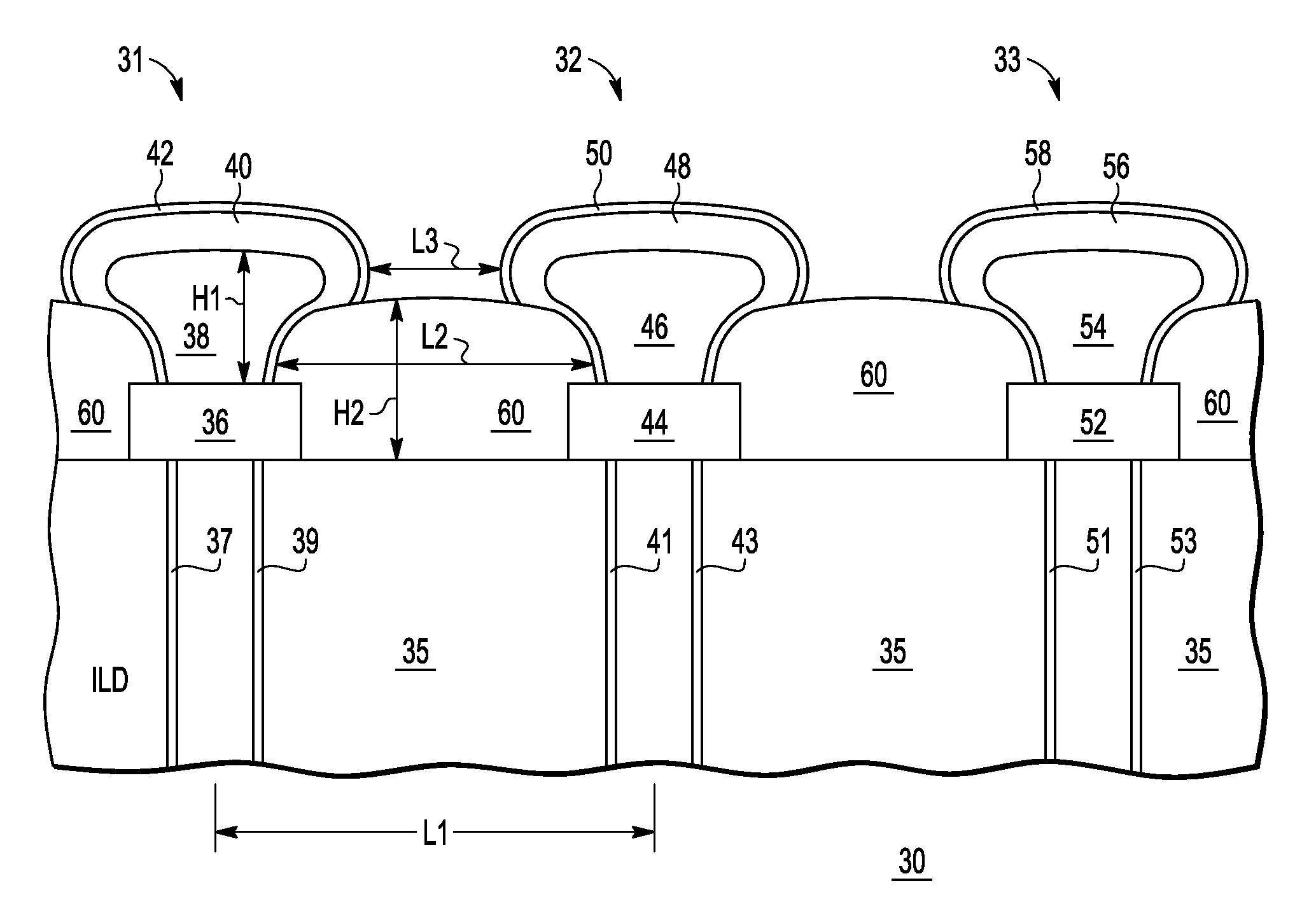
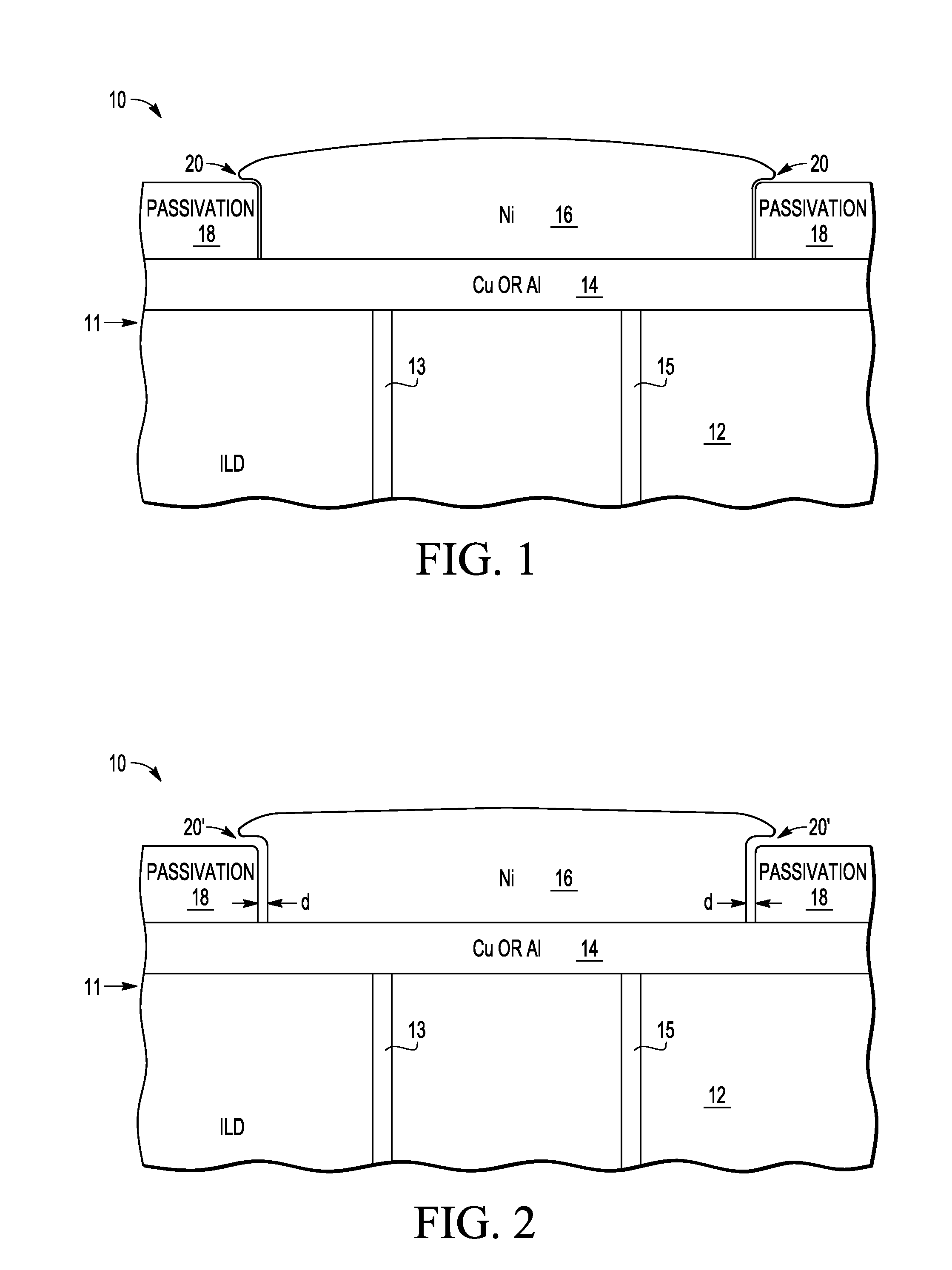
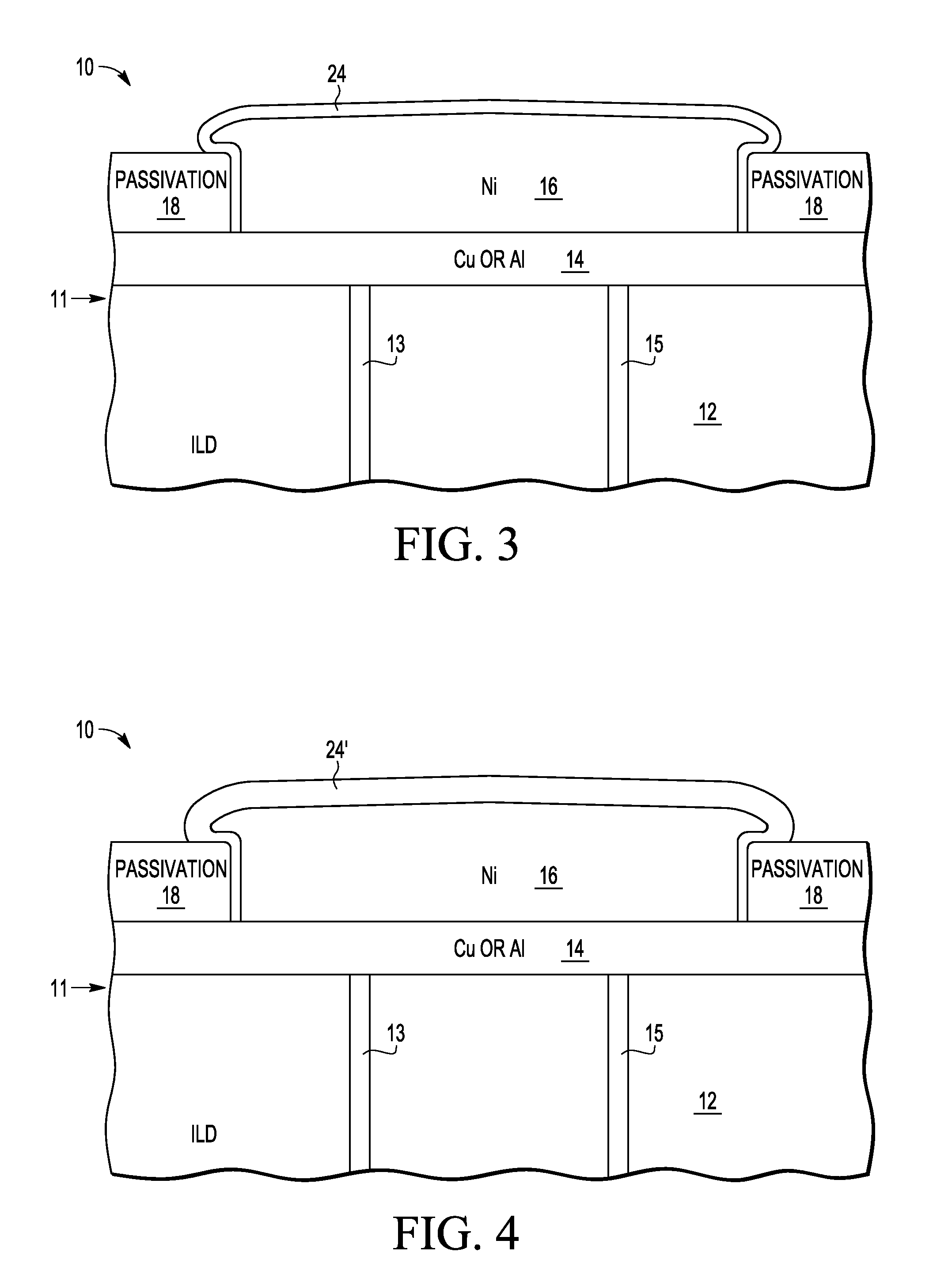
[0007]Illustrated in FIG. 1 is a cross-sectional view of a semiconductor device structure 10 which will minimize reliability issues associated with intermetallic compounds caused by prolonged operation at high operating temperatures. A patterned semiconductor die 11 generally has an inter-level dielectric (ILD) 12, an overlying conductive layer 14 and a patterned passivation layer 18. The patterned passivation layer 18 is an insulating, protective material and has an opening which exposes the conductive layer 14. In one form the conductive layer 14 is either copper or aluminum. Conductive paths or vias 13 and 15 are formed within the ILD 12 and electrically connect the conductive layer 14 to circuitry (not shown) underlying the ILD 12. The vias 13 and 15 in one embodiment are formed by patterning and etching the ILD 12. The vias 13 and 15 are filled with an electrically conductive material such as copper. It should be understood that any number of conductive vias may be implemented ...


PUM


Abstract

A semiconductor device structure has a semiconductor die that has a bond pad with a passivation layer surrounding a portion of the bond pad. A nickel layer, which is deposited, is on the inner portion. A space is between a sidewall of the nickel layer and the passivation layer and extends to the bond pad. A palladium layer is over the nickel layer and fills the space. The space is initially quite small but is widened by an isotropic etch so that when the palladium layer is deposited, the space is sufficiently large so that the deposition of palladium is able to fill the space. Filling the space results in a structure in which the palladium contacts the nickel layer, the passivation layer and the bond pad.

Description

FIELD OF THE INVENTION[0001]This invention relates generally to integrated circuits, and more specifically, to the manufacture of semiconductors having metal contacts.BACKGROUND OF THE INVENTION[0002]Semiconductors typically use metallic bond pads to make electrical connection to underlying circuitry. A metal of choice for bond pads has been and continues to be aluminum because of its reliable deposition and patterning properties. However, aluminum has relatively high resistivity as compared with other metals such as copper. However, bare copper bond pads are known to be susceptible to corrosion and generally not consistent with wiring processes such as traditional wirebonding. Copper bond pads with an aluminum cap have been proposed to overcome such difficulties. Alternatives to using such copper bond pads with coatings is to form bond pads from two or more metals, such as aluminum, gold, nickel, palladium and alloys thereof. Many wire bond structures however will not pass high tem...

Claims


Application Information

Patent Timeline
IPC IPC(8): H01L23/498H01L21/768
CPCH01L24/03H01L24/05H01L24/48H01L24/85H01L2224/04042H01L2224/05082H01L2224/05155H01L2224/05164H01L2224/05644H01L2224/45144H01L2224/45147H01L2224/48463H01L2224/4847H01L2224/85203H01L2224/85207H01L2924/01013H01L2924/01028H01L2924/01029H01L2924/01046H01L2924/01078H01L2924/01079H01L2924/01082H01L2924/01327H01L2924/14H01L2924/01033H01L2224/48644H01L2224/48844H01L2924/00014H01L2224/05027H01L2224/03831H01L2224/05124H01L2224/05147H01L2224/05007H01L2924/00H01L2224/45099H01L2924/00012
Inventor MATHEW, VARUGHESE
Owner NXP USA INC
Why Eureka
Try Eureka