Structure and fabricating method with self-aligned bit line contact to word line in split gate flash

Inactive Publication Date: 2005-01-06
TAIWAN SEMICON MFG CO LTD
View PDF11 Cites 0 Cited by
  • Summary
  • Abstract
  • Description
  • Claims
  • Application Information

AI Technical Summary

Benefits of technology

[0009] It is a primary objective of the invention to provide a split gate flash cell with self-aligned bit contact to word line. It is also a primary objective of the invention to provide a method of forming a split gate flash cell with self-aligned bit contact to word line through which a significant reduction in the split-gate flash cell area is possible.** As is well known in the art, a split-gate flash memory cell normally has source and drain regions that are contacted by utilizing poly plugs. Insulating layers are required as spacers to separate these poly plugs from the floating gates and control gates of the cell, and this use

Problems solved by technology

Furthermore, because of the high voltages required in the erase operation the s

Method used


Image

  • Structure and fabricating method with self-aligned bit line contact to word line in split gate flash
  • Structure and fabricating method with self-aligned bit line contact to word line in split gate flash
  • Structure and fabricating method with self-aligned bit line contact to word line in split gate flash

Examples


Embodiment Construction

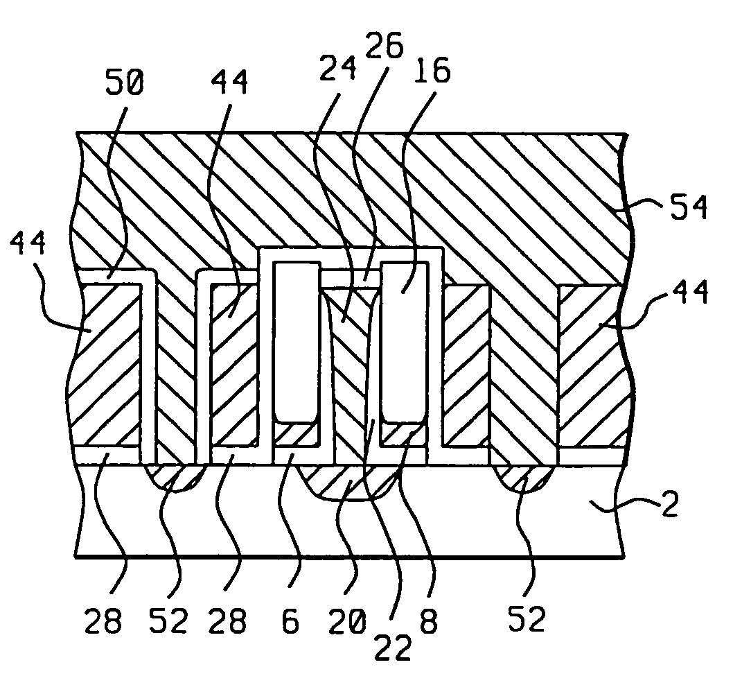
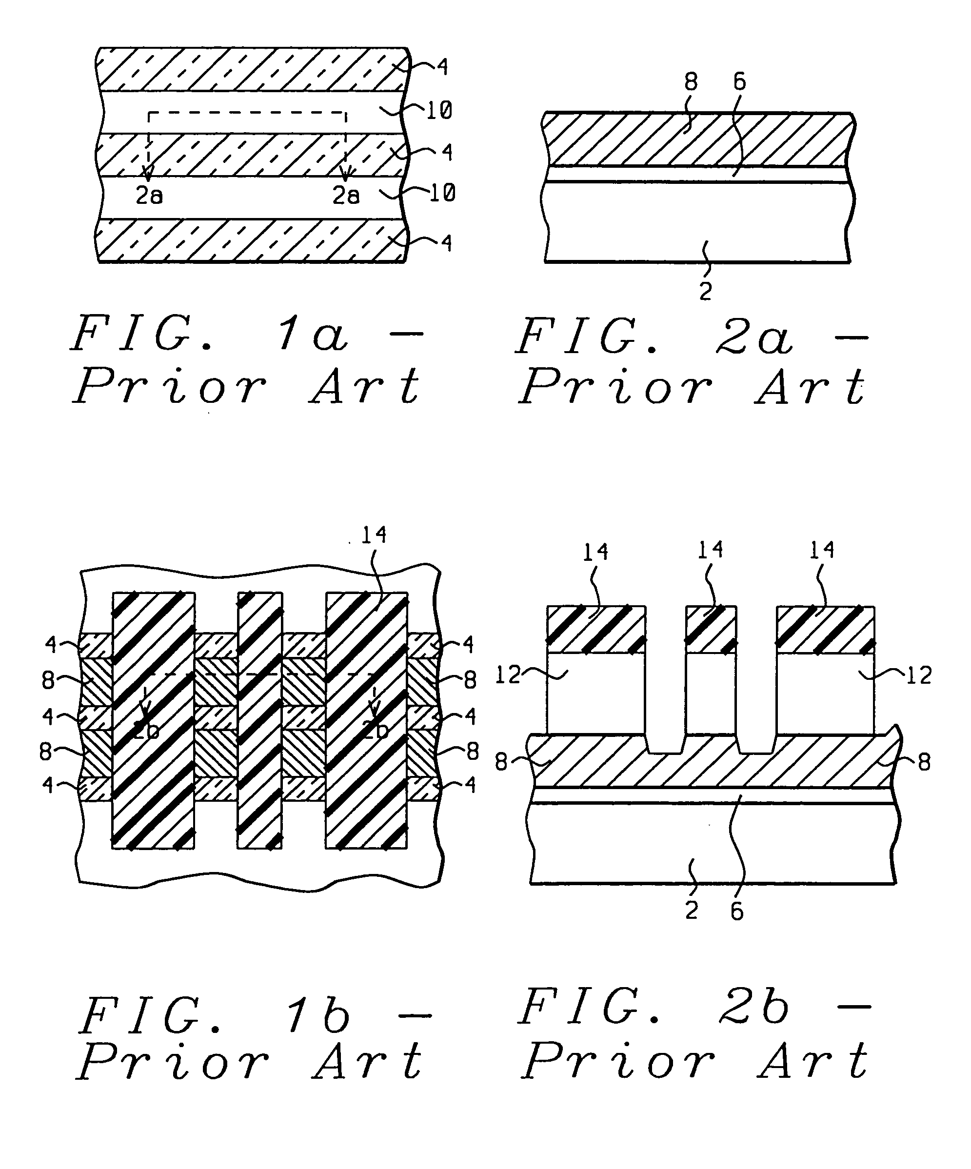
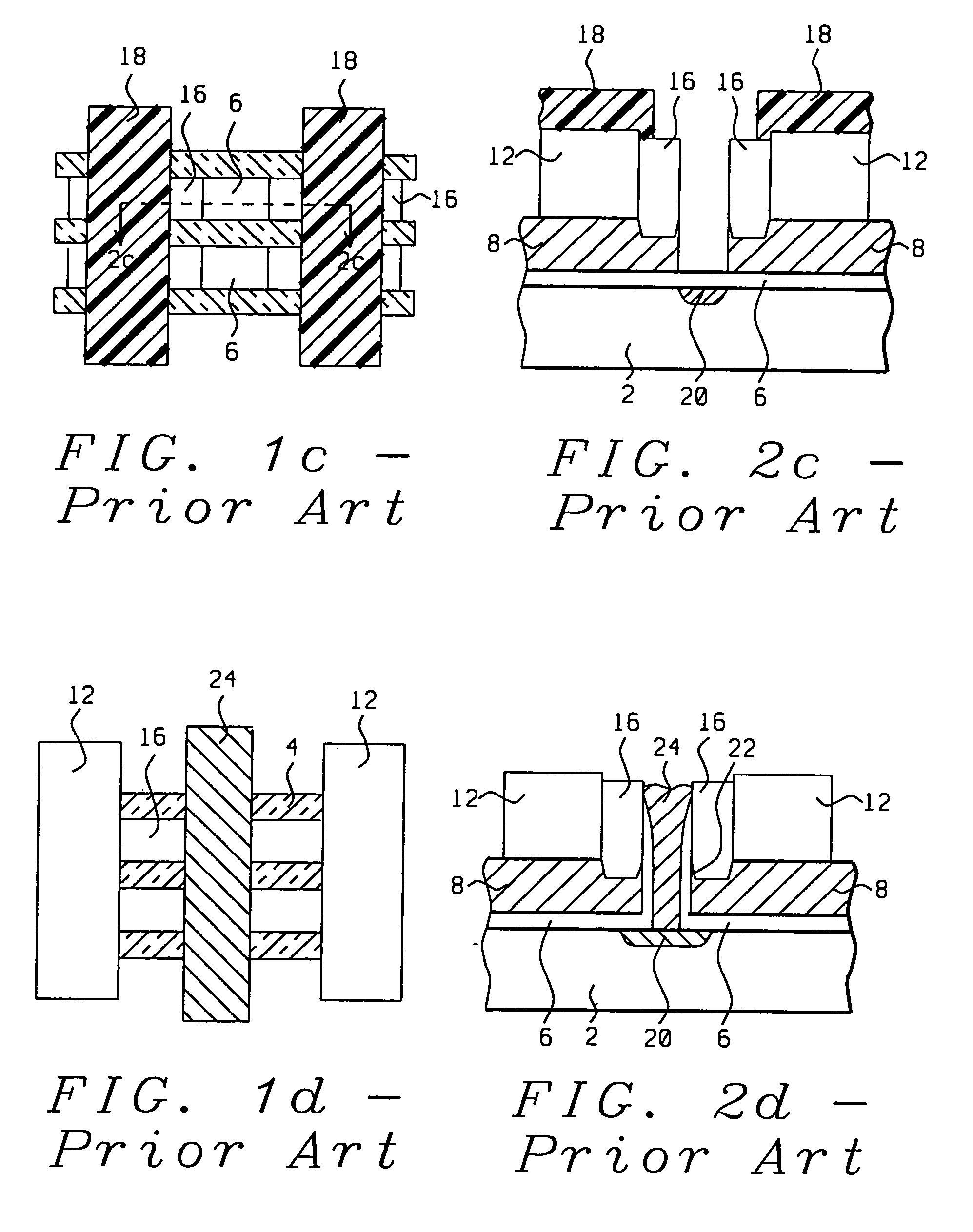
[0015] Preferred embodiments of the invention are well described with the aid of FIGS. 3a-3j and 4a-4j. A method of fabricating a novel split gate flash memory cell is presented in FIGS. 3a-6j, where top views of the cell are presented at successive stages of the process and in FIGS. 4a-4j, which show the corresponding cross-sections. A floating gate oxide, 6, is formed on a semiconductor substrate, 2, which preferably is a silicon substrate, to a thickness of about 80 Angstroms, followed by deposition of a poly 1 layer, 8, to a depth of about 800 Angstroms. Active regions, 10, are defined using isolating regions, such as shallow trench isolation regions, 4. This is followed by deposition of a nitride layer, which preferably is a silicon nitride layer to a depth of about 2500 Angstroms. A photoresist layer, 14, is then formed as shown in FIGS. 3b and 4b. The photoresist pattern, 14, is used in etching the silicon nitride layer to achieve the shape of region 12 of FIG. 4b. A poly 1 e...


PUM


Abstract

A new structure is disclosed for semiconductor devices in which contact regions are self-aligned to conductive lines. Openings to a gate oxide layer, in partially fabricated devices on a silicon substrate, have insulating sidewalls. First polysilicon lines disposed against the insulating sidewalls extend from below the top of the openings to the gate oxide layer. Oxide layers are grown over the top and exposed sides of the first polysilicon lines serving to insulate the first polysilicon lines. Polysilicon contact regions are disposed directly over and connect to silicon substrate regions through openings in the gate oxide layer and fill the available volume of the openings. Second polysilicon lines connect to the contact regions and are disposed over the oxide layers grown on the first polysilicon lines.

Description

BACKGROUND OF THE INVENTION [0001] (1) Field of the Invention [0002] The present invention relates generally to semiconductor integrated circuit technology and more particularly to split gate memory cells used in flash EPROMs (Electrically Erasable Programmable Read Only Memory). [0003] (2) Description of Prior Art [0004] Increased performance in computers is often directly related to a higher level of circuit integration. Tolerances play an important role in the ability to shrink dimensions on a chip. Self-alignment of components in a device serves to reduce tolerances and thus improve the packing density of chips. Other techniques can be important in shrinking device size. A method is disclosed later in the embodiments of the present invention of forming a structure with self-aligned bit line contact to word line through which a significant reduction in the area of the split gate flash cell is possible. [0005] As is well known in the art, split gate flash cells have bit lines and ...

Claims


Application Information

Patent Timeline
IPC IPC(8): H01L21/336H01L21/60H01L21/8242H01L21/8247H01L27/115H01L29/76
CPCH01L21/76897H01L27/11521H01L27/115H10B69/00H10B41/30
Inventor HSIEH, CHIA TA
Owner TAIWAN SEMICON MFG CO LTD
Why Eureka
Try Eureka