

Printed circuit board
a printed circuit board and circuit board technology, applied in the direction of printed circuits, electrical devices, printed circuit aspects, etc., can solve the problems of unavoidable mismatching of differential characteristic impedances at electrical length-adjusting portions, affecting the skew adjustment of conventional meander trace configuration, and reducing signal reflections, so as to reduce the deterioration of waveform quality due to skew adjustment, the effect of reducing the trace length of the whole skew-adjusting arrangemen
- Summary
- Abstract
- Description
- Claims
- Application Information
AI Technical Summary
Benefits of technology
Problems solved by technology
Method used
Image

Examples
first embodiment
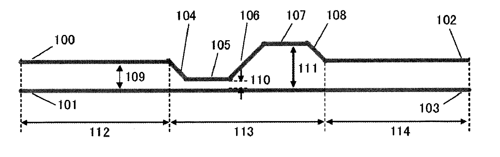
[0040]FIG. 1 is a front upper view illustrating a first embodiment of the present invention. A differential conductive trace pair on a printed circuit board is shown. Indicated by 112 and 114 are non-skew-adjusting portions which are not involved in a skew adjustment. Indicated by 113 is a skew-adjusting portion. The non-skew-adjusting portions have transmission lines 100 and 101 on a transmitter side. The non-skew-adjusting portions have transmission lines 102 and 103 on a receiver side. As shown, the transmission line 100 at the transmitting end is connected to the transmission line 102 at the receiving end by transmission line segments 104-108. Preferably, the bend angle for connecting the transmission lines or transmission line segments is equal to or less than 45 degrees. This also applies to embodiments (described later) other than the present embodiment. Spacings 109, 110, 111 indicate a spacing between the traces of the differential trace pair in the non-skew-adjusting porti...
second embodiment
[0053]FIG. 7 is a front upper view illustrating a second embodiment of the present invention. The figure shows a differential trace pair on a printed circuit board. Differential characteristic impedances are matched by bringing a trace for which a skew adjustment is not made closer to a trace for which a skew adjustment is made.
[0054]Indicated by 709 is a skew-adjusting portion. With respect to the trace for which a skew adjustment is made, a transmission line segment 100 at a transmitting end is connected to a transmission line segment 102 at a receiving end by transmission line segments 700-703. With respect to the trace for which a skew adjustment is not made, a transmission line segment 101 at the transmitting end is connected to a transmission line segment 103 at the receiving end by transmission line segments 704-706. A differential trace pair spacing 707 in the transmission line segment 701 is greater than the spacing 109. A differential trace pair spacing 708 in the transmis...
third embodiment
[0062]FIG. 11 is a front upper view illustrating a third embodiment of the present invention. The figure shows a differential trace pair on a printed circuit board. A differential characteristic impedance matching between a skew-matching portion 1108 and non-skew-adjusting portions 112, 114 is maintained by making use of the characteristic that the differential characteristic impedance varies according to trace width. As shown, with respect to a trace for which a skew adjustment is made, the transmission line segment 100 at the transmitting end is connected to the transmission line segment 102 at the receiving end by transmission line segments 1100-1103. A differential trace pair spacing 1106 of the convex transmission line segment 1101 is greater than the spacing 109. A differential trace pair spacing 1107 of the concave transmission line segment 1103 is smaller than the spacing 109. In a skew-adjusting portion 1108, the trace width of the convex transmission line segment 1101 is g...
PUM
 Abstract
Description
Claims
Application Information