Efficient High Voltage Switching Circuits and Monolithic Integration of Same

a high-voltage switching circuit and monolithic technology, applied in the direction of electronic switching, pulse technique, transistors, etc., can solve the problems of power loss within the semiconductor device, high breakdown voltage at the expense of performance capability, and become increasingly importan

Active Publication Date: 2011-09-01
INFINEON TECH AMERICAS CORP
View PDF101 Cites 56 Cited by
  • Summary
  • Abstract
  • Description
  • Claims
  • Application Information

AI Technical Summary

Benefits of technology

[0007]The present invention is directed to efficient high voltage switching circuits and monolithic integration of same, substant

Problems solved by technology

As the performance requirements placed on modern electronic systems grow ever more stringent, power losses within a semiconductor device, as well as factors affecting switch

Method used


Image

  • Efficient High Voltage Switching Circuits and Monolithic Integration of Same
  • Efficient High Voltage Switching Circuits and Monolithic Integration of Same
  • Efficient High Voltage Switching Circuits and Monolithic Integration of Same

Examples


Embodiment Construction

[0015]The present invention is directed to efficient high voltage switching circuits and monolithic integration of same. The following description contains specific information pertaining to the implementation of the present invention. One skilled in the art will recognize that the present invention may be implemented in a manner different from that specifically discussed in the present application. Moreover, some of the specific details of the invention are not discussed in order not to obscure the invention.

[0016]The drawings in the present application and their accompanying detailed description are directed to merely exemplary embodiments of the invention. To maintain brevity, other embodiments of the present invention are not specifically described in the present application and are not specifically illustrated by the present drawings.

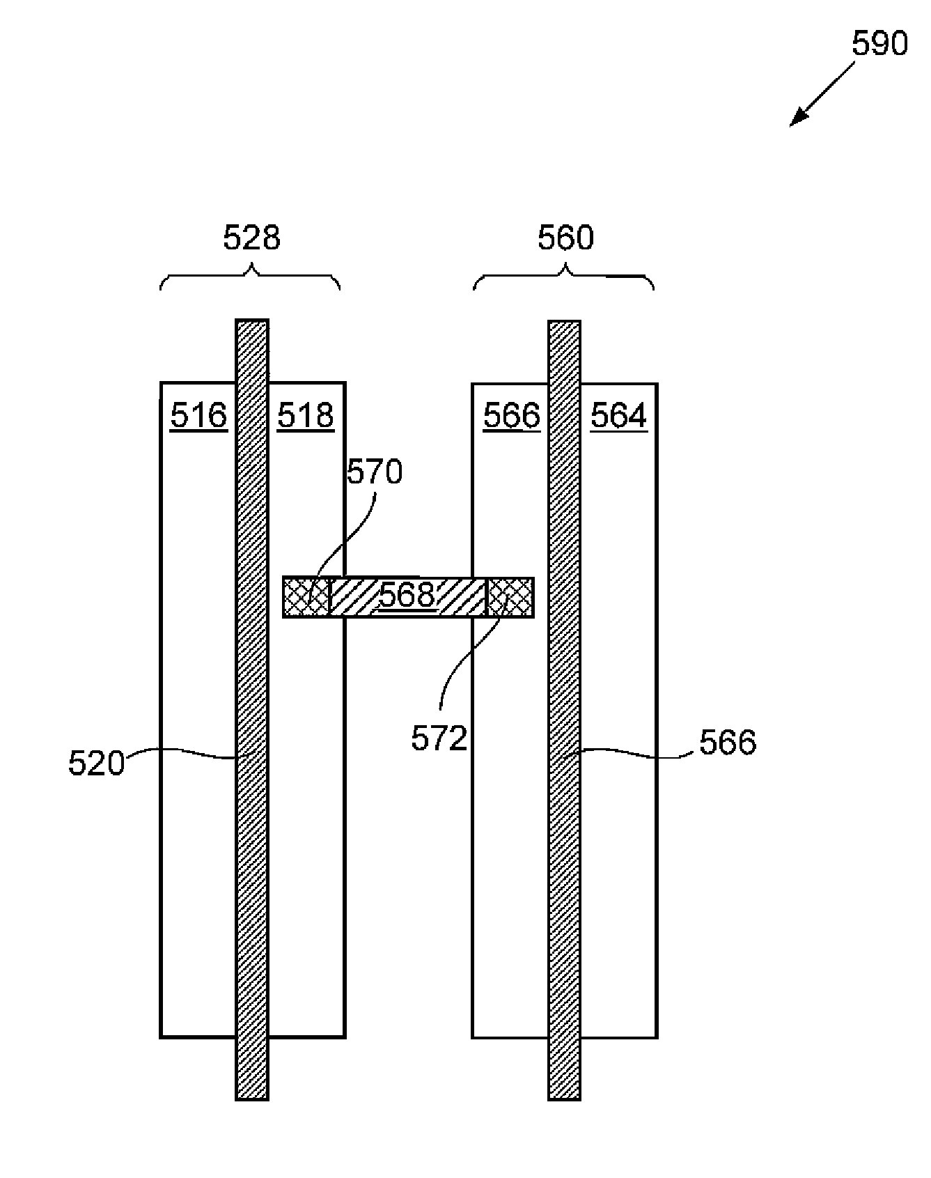
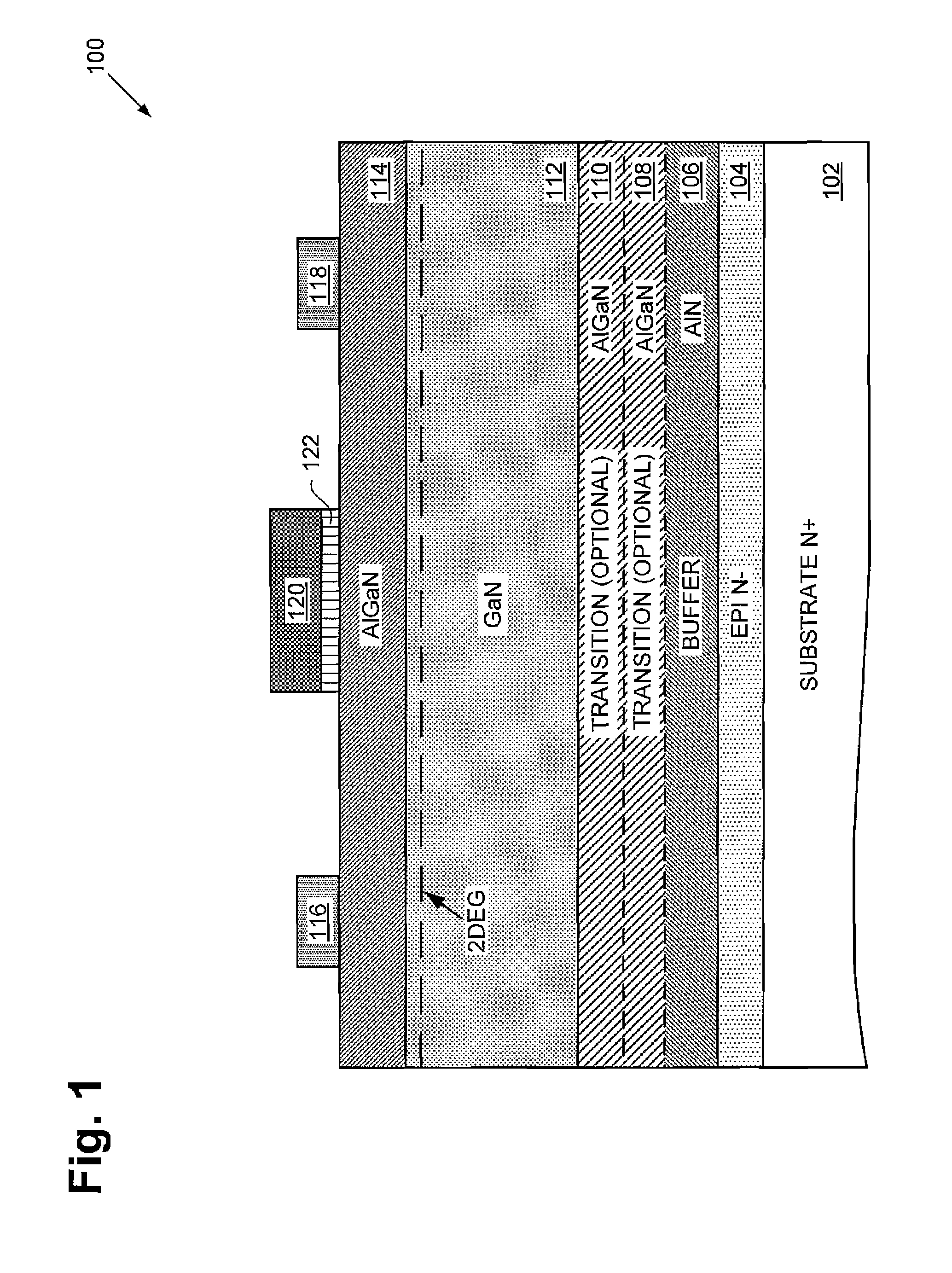
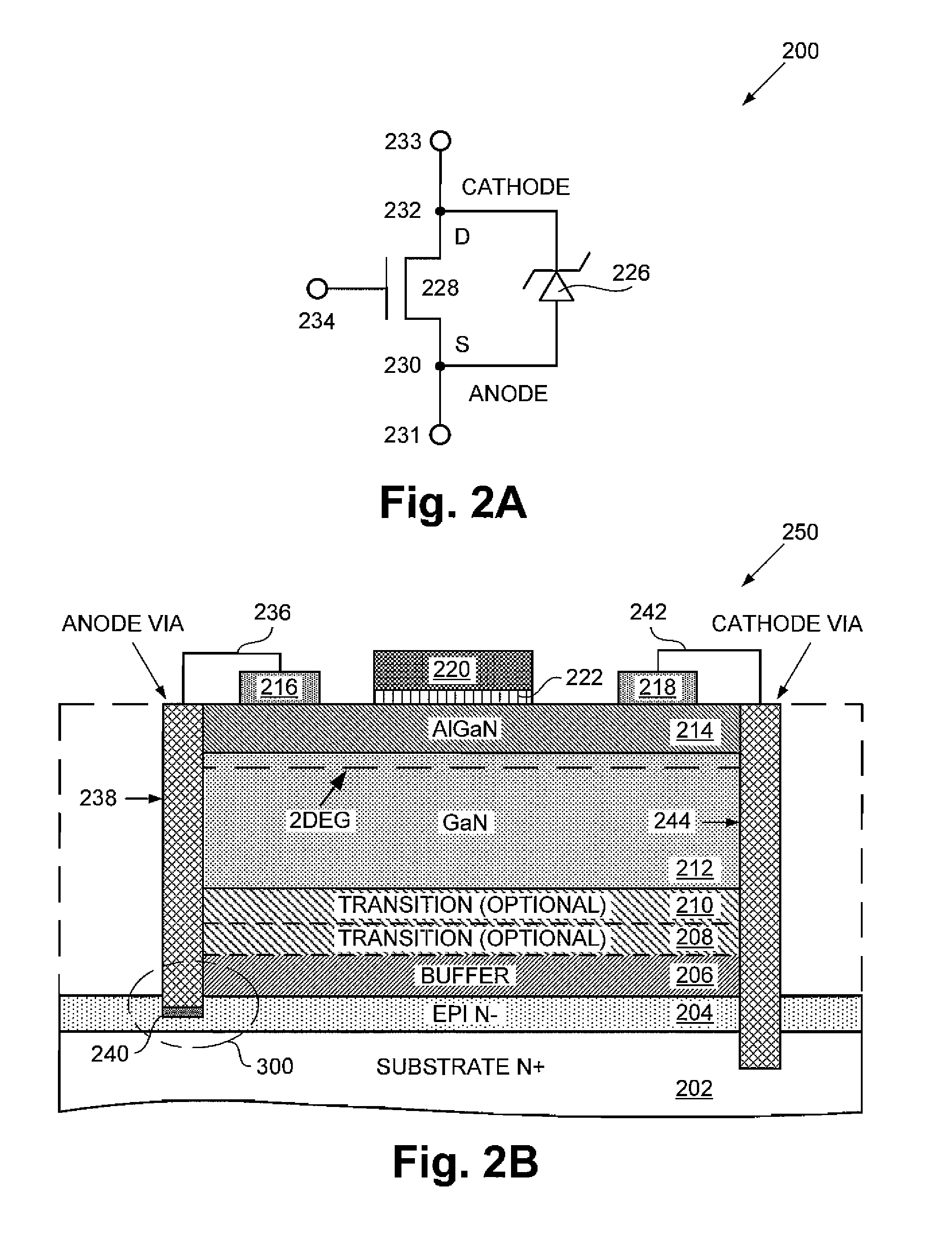
[0017]FIG. 1 shows a cross-sectional view of exemplary group III-V semiconductor device 100, and more particularly a III-Nitride high electron mob...


PUM


Abstract

A high voltage switching circuit includes first and second group III-V transistors, the second group III-V transistor having a greater breakdown voltage than the first group III-V transistor. The circuit further includes a silicon diode in a parallel arrangement with the first group III-V transistor, the parallel arrangement being in cascade with the second group III-V transistor. The circuit is effectively a three-terminal device, where a first terminal is coupled to a gate of the second III-V transistor, a source of the first III-V transistor, and an anode of the silicon diode. A second terminal is coupled to a gate of the first group III-V transistor, and a third terminal is coupled to a drain of the second group III-V transistor. The first group III-V transistor might be an enhancement mode transistor. The second group III-V transistor might be a depletion mode transistor. The first and second group III-V transistors can be GaN HEMTs.

Description

[0001]The present application claims the benefit of and priority to a pending provisional application entitled “Monolithic Integration of Silicon and Group III-V Devices and Efficient Circuits Utilizing Same,” Ser. No. 61 / 339,190 filed on Mar. 1, 2010. The disclosure in that pending provisional application is hereby incorporated fully by reference into the present application.BACKGROUND OF THE INVENTIONDefinition[0002]In the present application, “group III-V semiconductor” or “group III-V device” or similar terms refers to a compound semiconductor that includes at least one group III element and at least one group V element, such as, but not limited to, gallium nitride (GaN), gallium arsenide (GaAs), indium aluminum gallium nitride (InAlGaN), indium gallium nitride (InGaN) and the like. Analogously, “III-nitride semiconductor” refers to a compound semiconductor that includes nitrogen and at least one group III element, such as, but not limited to, GaN, AlGaN, InN, AlN, InGaN, InAlGa...

Claims


Application Information

Patent Timeline
IPC IPC(8): H01L27/06
CPCH01L27/0605H01L29/2003H01L29/7787H01L27/0883H01L21/8258H01L27/0629H03K17/567
Inventor BRIERE, MICHAEL A.
Owner INFINEON TECH AMERICAS CORP
Why Eureka
Try Eureka