Integrated circuit

a technology of integrated circuits and memory devices, applied in the field of semiconductor memory device design technology, can solve the problems of internal circuits that may not perform normal initialization operations, internal circuits that are often exposed to noise, and affect so as to prevent noise and not degrade the yield of semiconductor memory devices

Inactive Publication Date: 2011-09-01
SK HYNIX INC
View PDF7 Cites 0 Cited by
  • Summary
  • Abstract
  • Description
  • Claims
  • Application Information

AI Technical Summary

Benefits of technology

[0023]Exemplary embodiments of the present invention are directed to an integrated circuit that is robust against noise and does not degrade the yield of a semiconductor memory device.

Problems solved by technology

Meanwhile, the reset signal RESETB applied to the pad 110 is frequently exposed to noise.
Thus, this may cause a malfunction due to the unintended initialization of the internal circuit.
In this case, the internal circuit may fail to perform a normal initialization operation.
However, the known method has a limitation in that it may affect the yield of a semiconductor memory device.

Method used


Image

  • Integrated circuit
  • Integrated circuit
  • Integrated circuit

Examples


Embodiment Construction

[0031]Exemplary embodiments of the present invention will be described below in more detail with reference to the accompanying drawings. The present invention may, however, be embodied in different forms and should not be construed as limited to the embodiments set forth herein. Rather, these embodiments are provided so that this disclosure will be thorough and complete, and will fully convey the scope of the present invention to those skilled in the art. Throughout the disclosure, like reference numerals refer to like parts throughout the various figures and embodiments of the present invention.

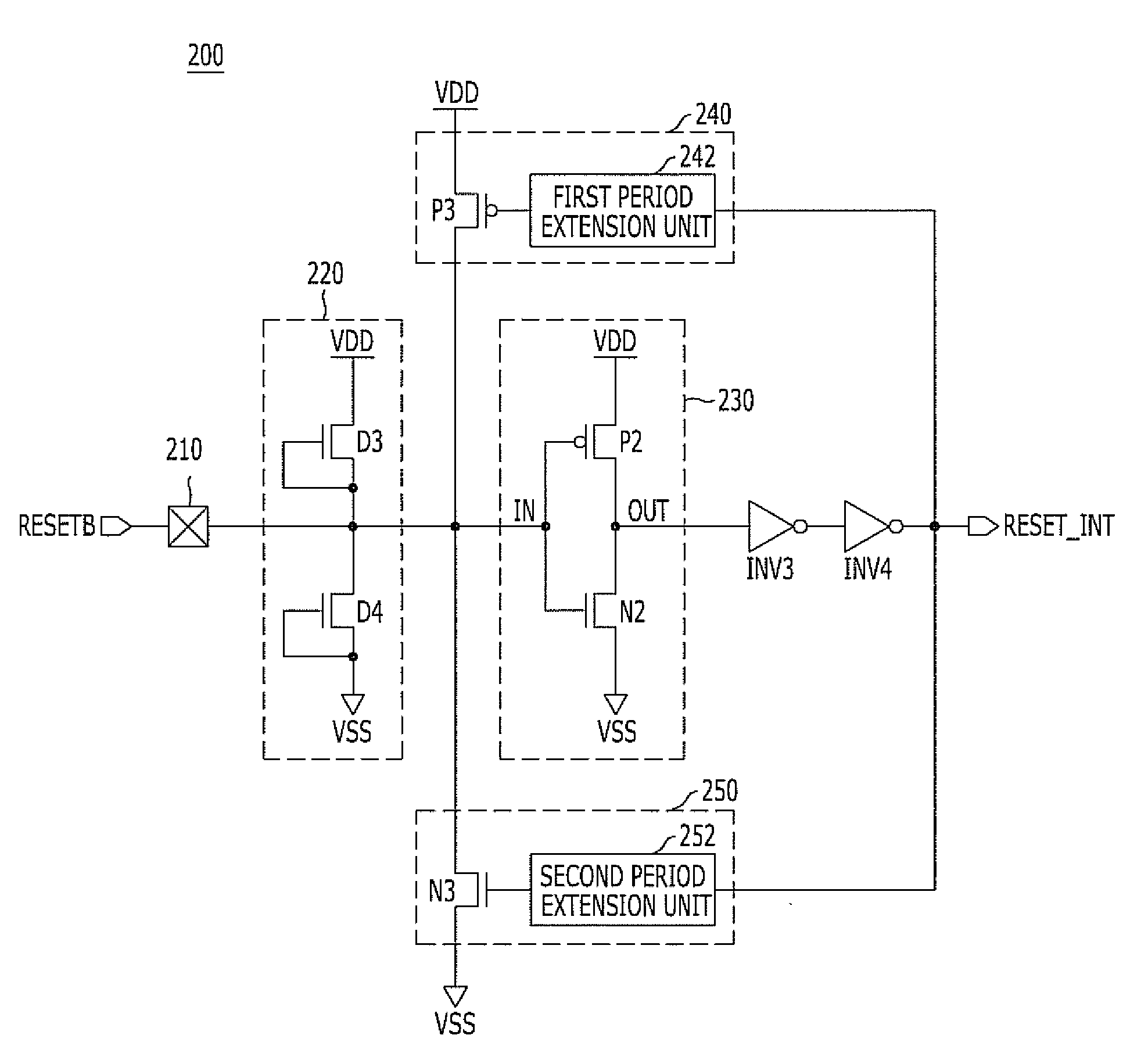
[0032]FIG. 5 is a block diagram of an integrated circuit in accordance with an exemplary embodiment of the present invention.

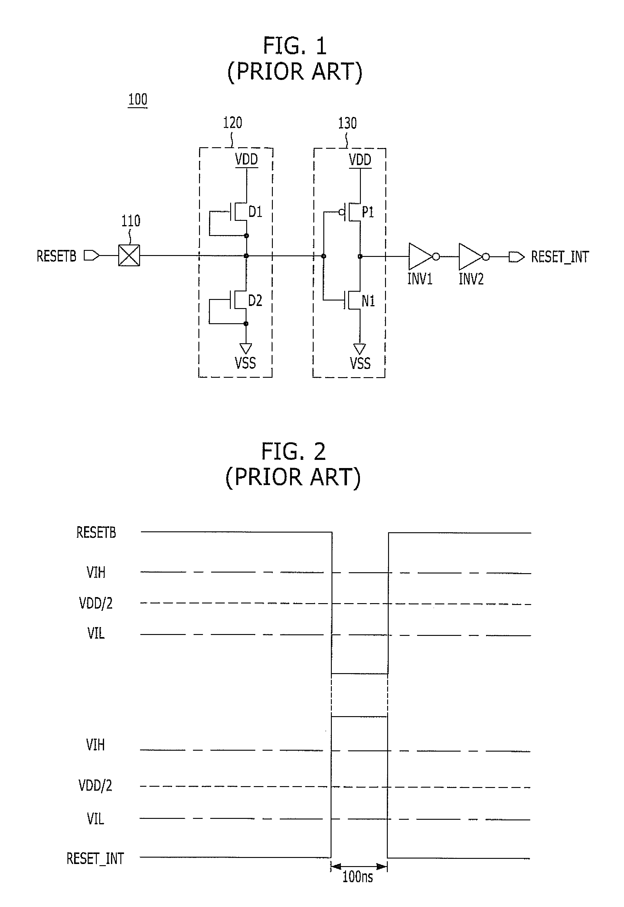
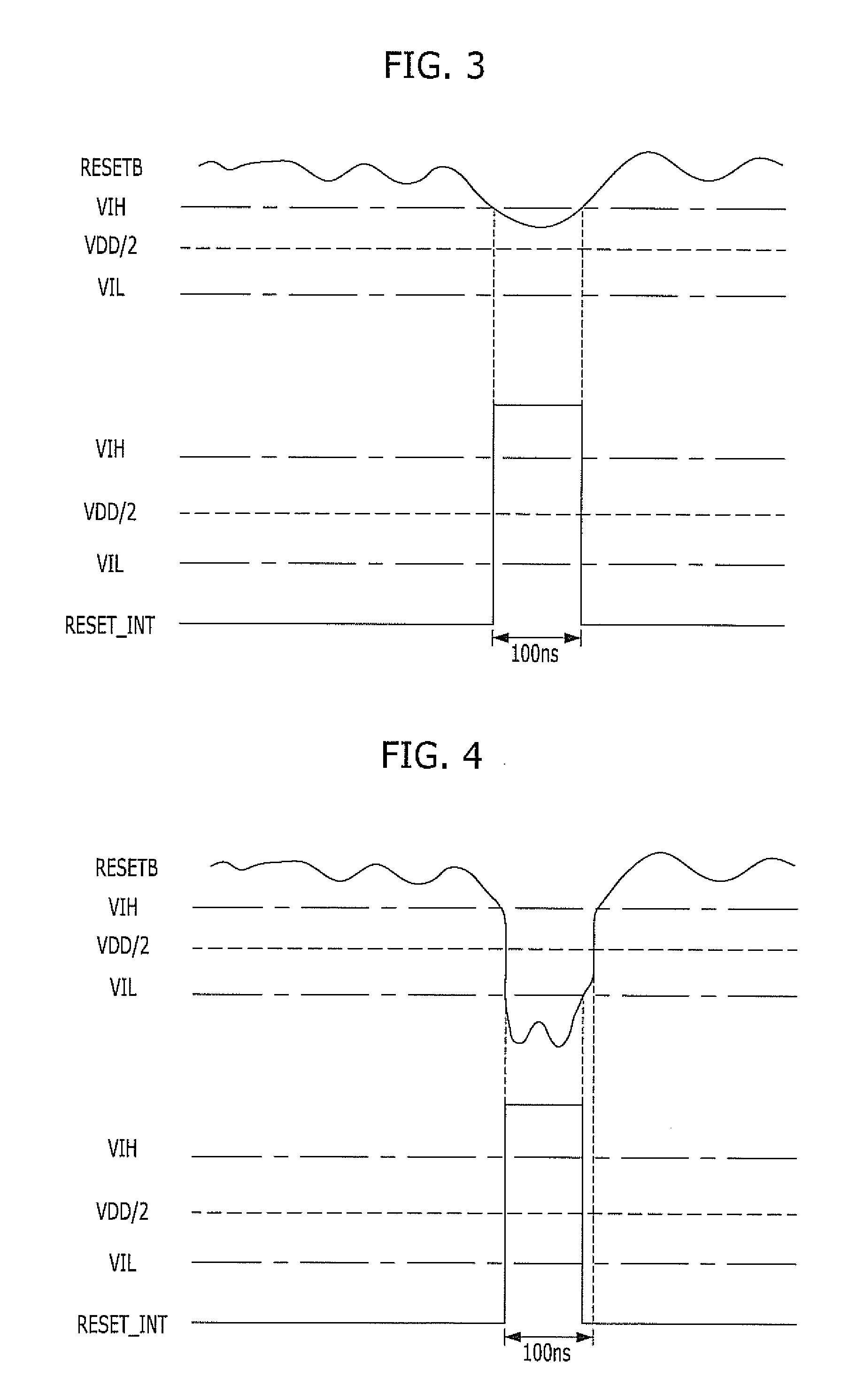
[0033]Referring to FIG. 5, an integrated circuit 200 in accordance with an exemplary embodiment of the present invention includes a pad 210, an electrostatic discharge (ESD) protection unit 220, an input buffer unit 230, a first inverter INV3, a second inverter INV4, a...


PUM


Abstract

An integrated circuit includes a pad, an input buffer unit, and a supplementary driving unit. The pad is configured to receive a reset signal from an external device. The input buffer unit is configured to buffer a reset signal applied to the pad. The supplementary driving unit is configured to receive an output signal from the input buffer unit and supplementarily drive an input terminal of the input buffer unit to a deactivation level of the reset signal.

Description

CROSS-REFERENCE(S) TO RELATED APPLICATIONS[0001]The present application claims priority of Korean Patent Application No. 10-2010-0018114, filed on Feb. 26, 2010, which is incorporated herein by reference in its entirety.BACKGROUND OF THE INVENTION[0002]Exemplary embodiments of the present invention relate to semiconductor design technology, and more particularly, to integrated circuits.[0003]A recent trend is to fabricate an integrated circuit such as a dynamic random access memory (DRAM) to have a low power consumption. Accordingly, the integrated circuit receives a reset signal from an external device. Herein, the reset signal is applied to initialize various internal circuits of the integrated circuit. Typically, the reset signal is a low active signal and is called a reset bar signal.[0004]FIG. 1 is a block diagram of a known integrated circuit.[0005]Referring to FIG. 1, an integrated circuit 100 includes a pad 110, an electrostatic discharge (ESD) protection unit 120, an input ...

Claims


Application Information

Patent Timeline
Patent Type & Authority Applications(United States)
IPC IPC(8): H03L7/00
CPCG11C7/109G11C11/4072G11C7/20H03K17/145H03K19/0185
Inventor PARK, KEE-TEOK
Owner SK HYNIX INC
Why Eureka
Try Eureka