Conformal layers by radical-component CVD

a radical component and radical technology, applied in the field of radical component cvd conformal layer, can solve the problems of dielectric material, dielectric material, structural features of the device having decreased spatial dimensions, etc., and achieve the effects of less volume shrinkage, less pore formation, and improved wetting properties

Active Publication Date: 2011-09-08
APPLIED MATERIALS INC
View PDF102 Cites 226 Cited by
  • Summary
  • Abstract
  • Description
  • Claims
  • Application Information

AI Technical Summary

Benefits of technology

[0005]Methods, materials, and systems are described for forming conformal dielectric layers containing silicon and nitrogen (e.g., a silicon-nitrogen-hydrogen (Si—N—H) film) from a carbon-free silicon-and-nitrogen precursor and radical-nitrogen precursor. The carbon-free silicon-and-nitrogen precursor is predominantly excited by contact with the radical-nitrogen precursor. Because the silicon-and-nitrogen film is formed without carbon, the conversion of the film into hardened silicon oxide is done with less pore formation and less volume shrinkage. The deposited silicon-and-nitrogen-containing film may be wholly or partially converted to silicon oxide which allows the optical properties of the conformal dielectric layer to be selectable. The deposition of a thin silicon-and-nitrogen-containing film may be performed at low temperature to form a liner layer in a substrate trench. The low temperature liner layer has been found to improve the wetting properties and allows flowable films to more completely fill the trench.

Problems solved by technology

The decreasing feature sizes result in structural features on the device having decreased spatial dimensions.
The widths of gaps and trenches on the device narrow to a point where the aspect ratio of gap depth to its width becomes high enough to make it challenging to fill the gap with dielectric material.
The depositing dielectric material is prone to clog at the top before the gap completely fills, producing a void or seam in the middle of the gap.

Method used


Image

  • Conformal layers by radical-component CVD
  • Conformal layers by radical-component CVD
  • Conformal layers by radical-component CVD

Examples


Embodiment Construction

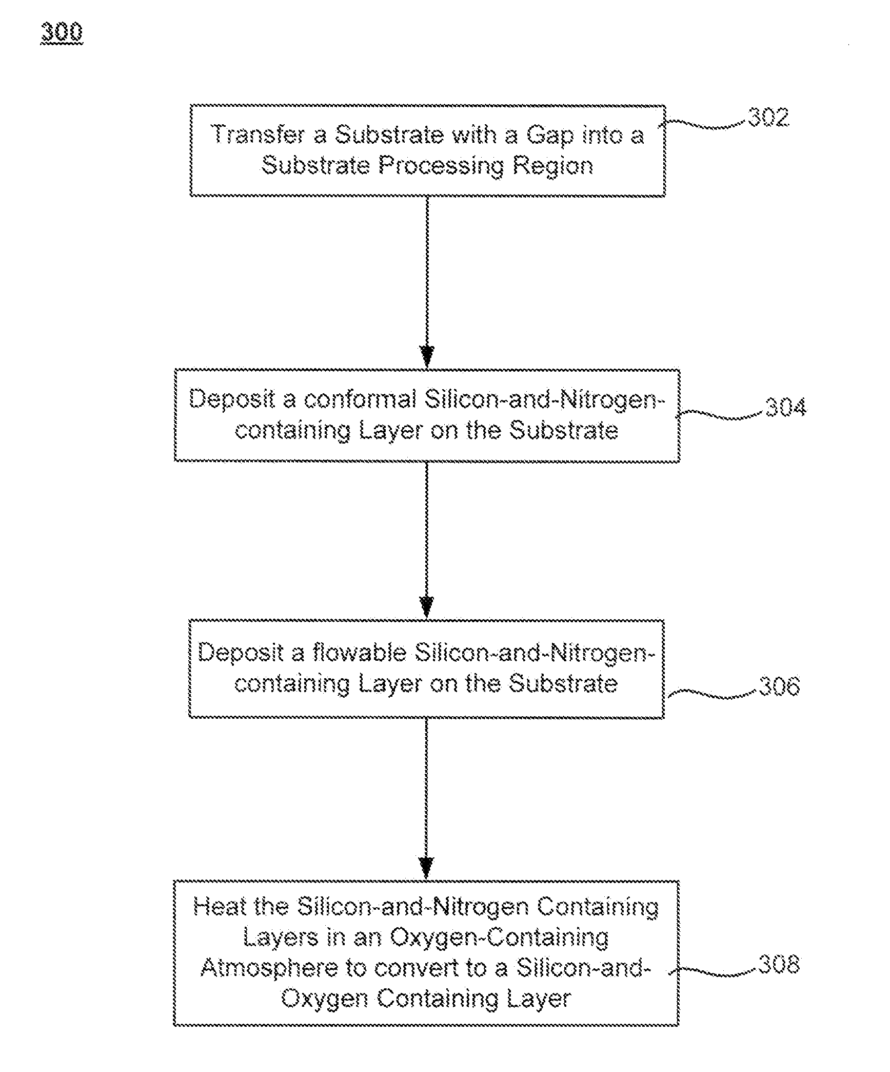
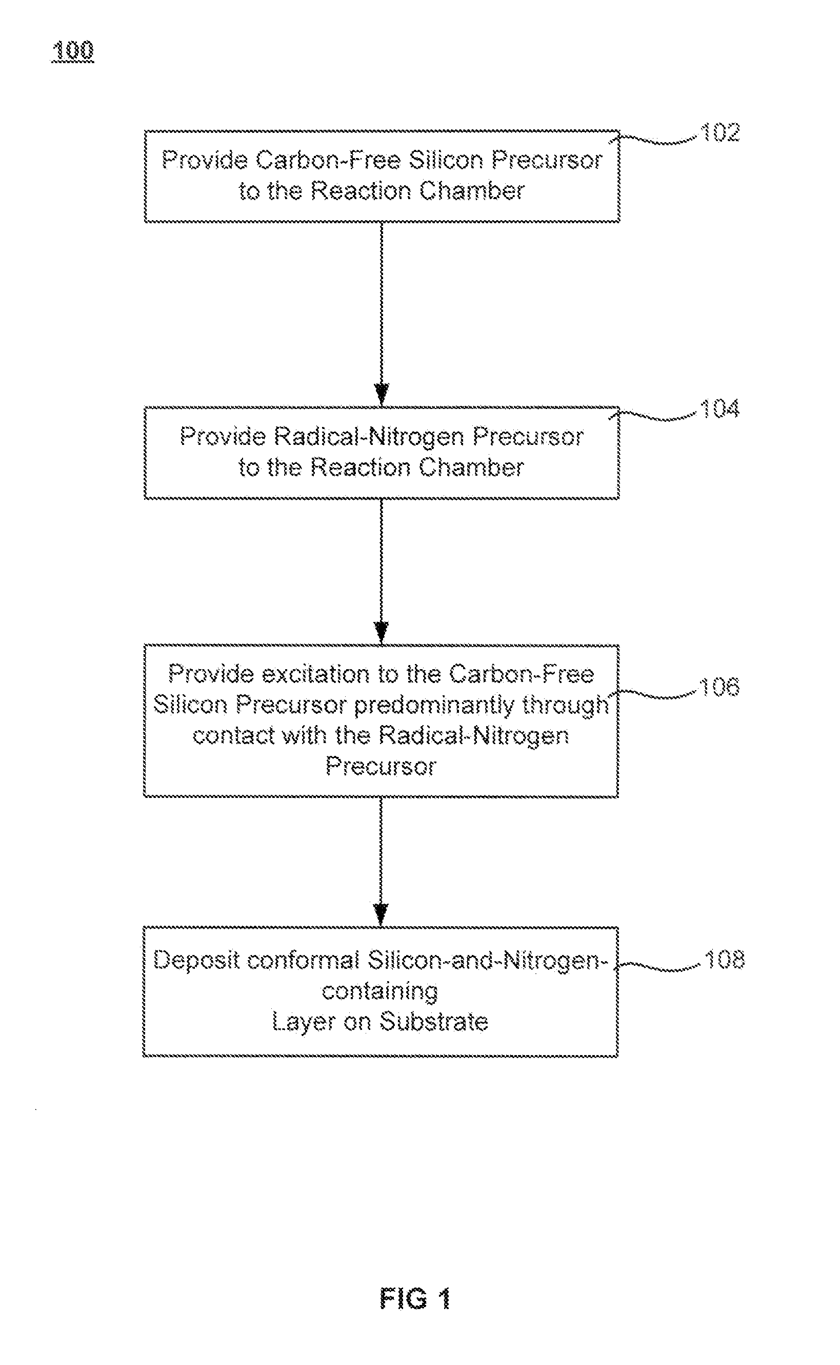
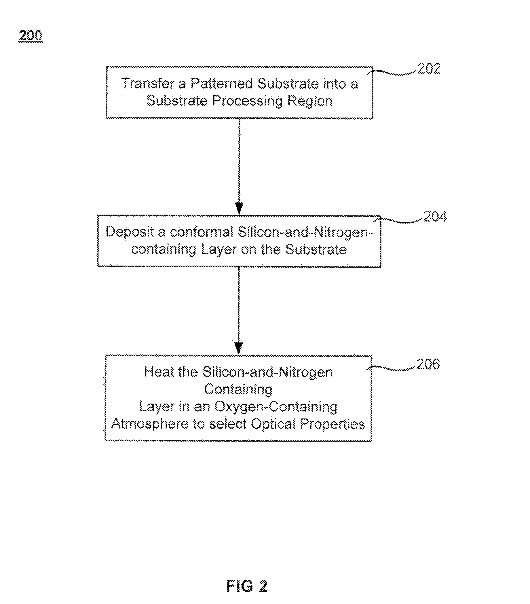
[0016]Methods, materials, and systems are described for forming conformal dielectric layers containing silicon and nitrogen (e.g., a silicon-nitrogen-hydrogen (Si—N—H) film) from a carbon-free silicon-and-nitrogen precursor and radical-nitrogen precursor. The carbon-free silicon-and-nitrogen precursor is predominantly excited by contact with the radical-nitrogen precursor. Because the silicon-and-nitrogen film is formed without carbon, the conversion of the film into hardened silicon oxide is done with less pore formation and less volume shrinkage. The deposited silicon-and-nitrogen-containing film may be wholly or partially converted to silicon oxide which allows the optical properties of the conformal dielectric layer to be selectable. The deposition of a thin silicon-and-nitrogen-containing film may be performed at low temperature to form a liner layer in a substrate trench. In embodiments, low temperature liner layers have been found to improve the wetting properties and allow f...


PUM

PropertyMeasurementUnit
pressureaaaaaaaaaa
temperatureaaaaaaaaaa
thicknessaaaaaaaaaa

Abstract

Methods, materials, and systems are described for forming conformal dielectric layers containing silicon and nitrogen (e.g., a silicon-nitrogen-hydrogen (Si—N—H) film) from a carbon-free silicon-and-nitrogen precursor and radical-nitrogen precursor. The carbon-free silicon-and-nitrogen precursor is predominantly excited by contact with the radical-nitrogen precursor. Because the silicon-and-nitrogen film is formed without carbon, the conversion of the film into hardened silicon oxide is done with less pore formation and less volume shrinkage. The deposited silicon-and-nitrogen-containing film may be wholly or partially converted to silicon oxide which allows the optical properties of the conformal dielectric layer to be selectable. The deposition of a thin silicon-and-nitrogen-containing film may be performed at low temperature to form a liner layer in a substrate trench. The low temperature liner layer has been found to improve the wetting properties and allows flowable films to more completely fill the trench.

Description

CROSS-REFERENCES TO RELATED APPLICATIONS[0001]This application claims the benefit of U.S. patent application Ser. No. 12 / 840,768 filed Jul. 21, 2010, and titled “FORMATION OF SILICON OXIDE USING NON-CARBON FLOWABLE CVD PROCESSES” and U.S. Prov. Pat. App. No. 61 / 311,061 filed Mar. 5, 2010, and titled “CONFORMAL LAYERS BY RADICAL-COMPONENT CVD.” The entire contents of these applications are incorporated herein by reference for all purposes.BACKGROUND OF THE INVENTION[0002]Semiconductor device geometries have dramatically decreased in size since their introduction several decades ago. Modern semiconductor fabrication equipment routinely produces devices with 45 nm, 32 nm, and 28 nm feature sizes, and new equipment is being developed and implemented to make devices with even smaller geometries. The decreasing feature sizes result in structural features on the device having decreased spatial dimensions. The widths of gaps and trenches on the device narrow to a point where the aspect rati...

Claims


Application Information

Patent Timeline
Patent Type & Authority Applications(United States)
IPC IPC(8): H01L21/31
CPCC23C16/345C23C16/452C23C16/56H01L21/76837H01L21/0217H01L21/02271H01L21/02326H01L21/02164
Inventor LIANG, JINGMEICHEN, XIAOLINLI, DONGQINGINGLE, NITIN K.
Owner APPLIED MATERIALS INC
Why Eureka
Try Eureka