Programmable III-Nitride Transistor with Aluminum-Doped Gate

a technology of iii-nitride and gate, applied in the field of semiconductor devices based on iiinitride, can solve the problems that iii-nitride heterojunction devices can introduce problems when used in power applications

Active Publication Date: 2011-09-22
INFINEON TECH AMERICAS CORP
View PDF5 Cites 32 Cited by
  • Summary
  • Abstract
  • Description
  • Claims
  • Application Information

AI Technical Summary

Benefits of technology

[0008]The present application is directed to a programmable III-nitride transistor with aluminum-doped gate, substantiall

Problems solved by technology

III-nitride heterojunction devices are desirable for power applications due to relatively high breakdown voltage, high current density, and low “on re

Method used


Image

  • Programmable III-Nitride Transistor with Aluminum-Doped Gate
  • Programmable III-Nitride Transistor with Aluminum-Doped Gate
  • Programmable III-Nitride Transistor with Aluminum-Doped Gate

Examples


Embodiment Construction

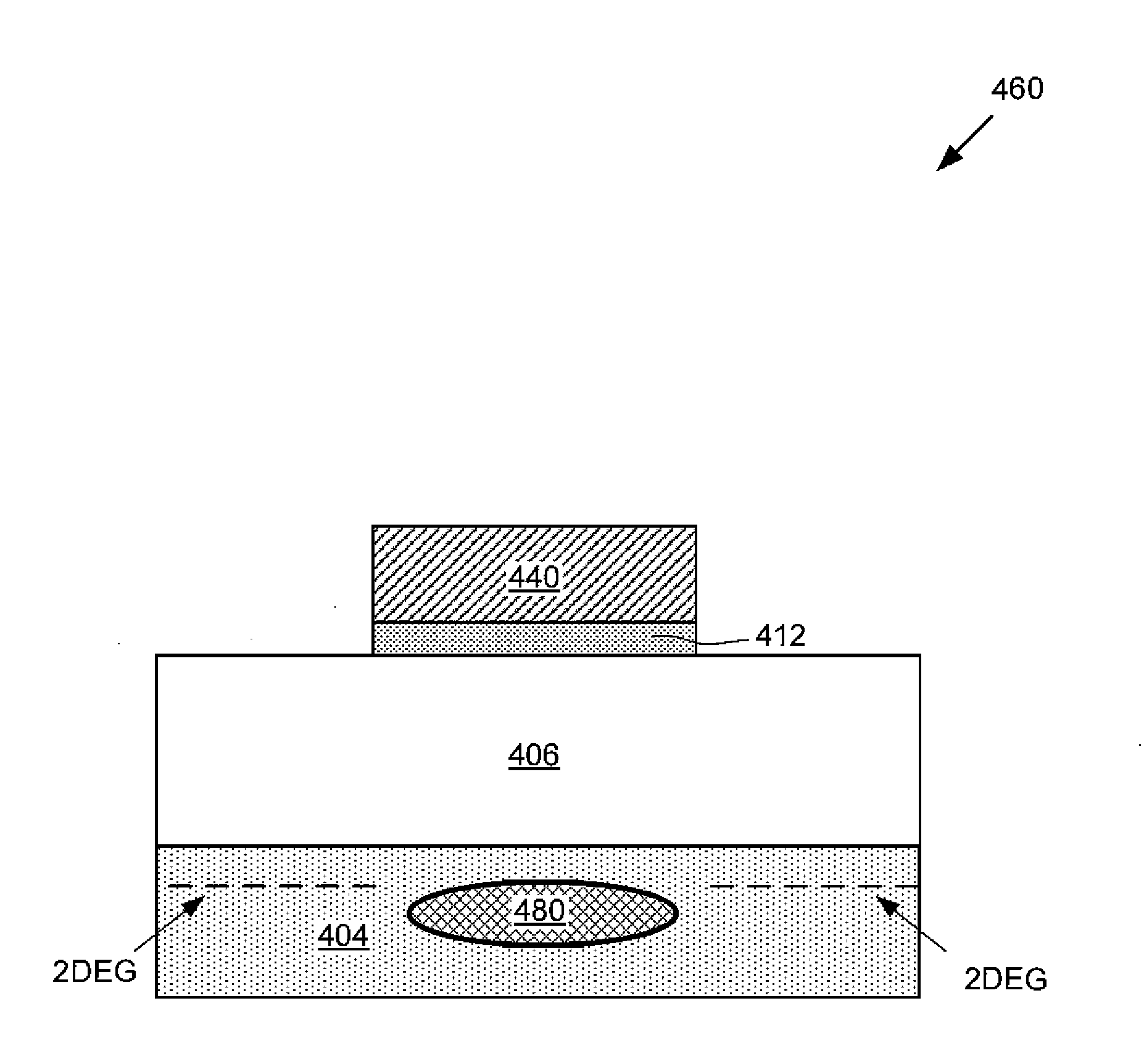
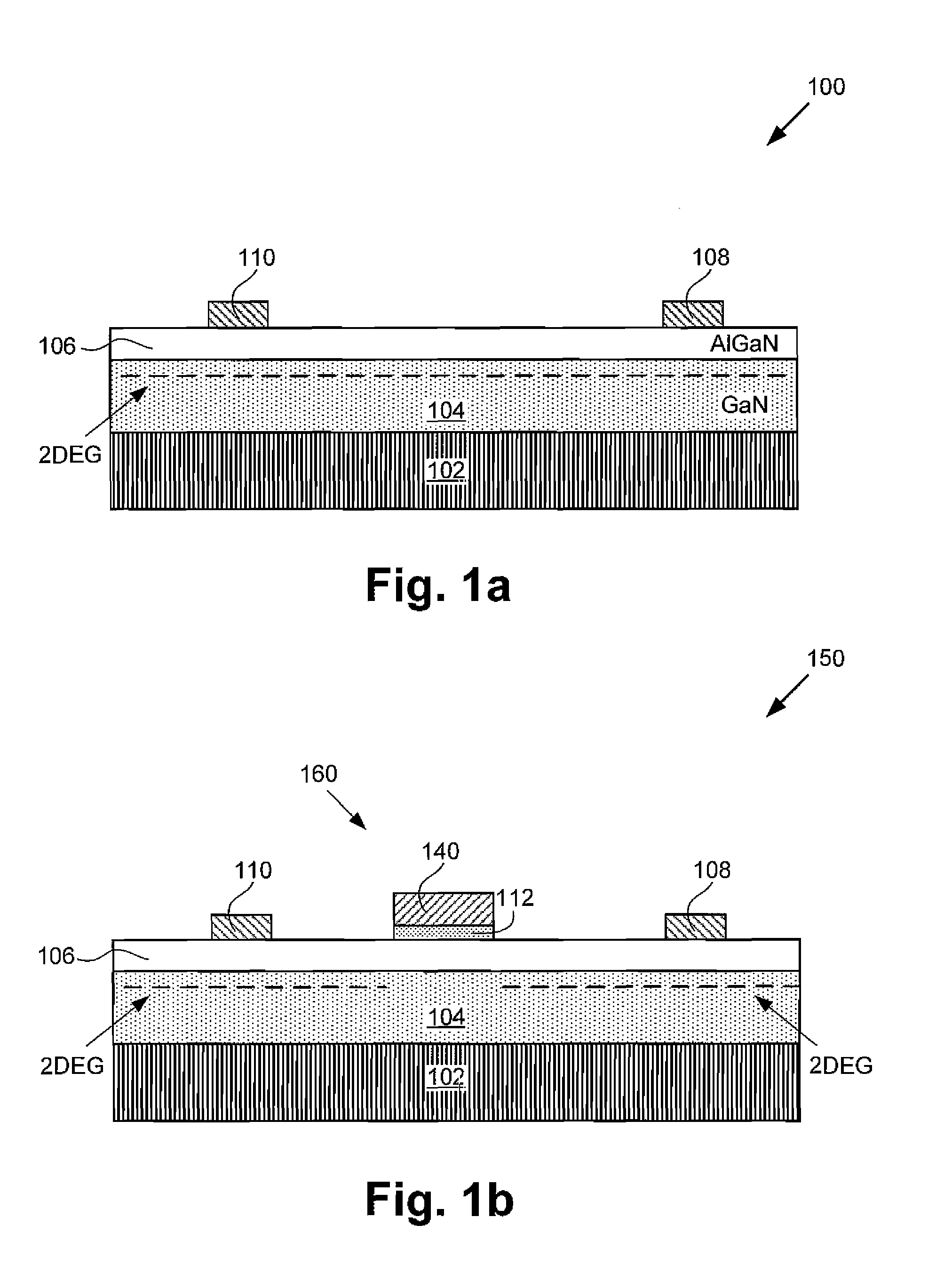
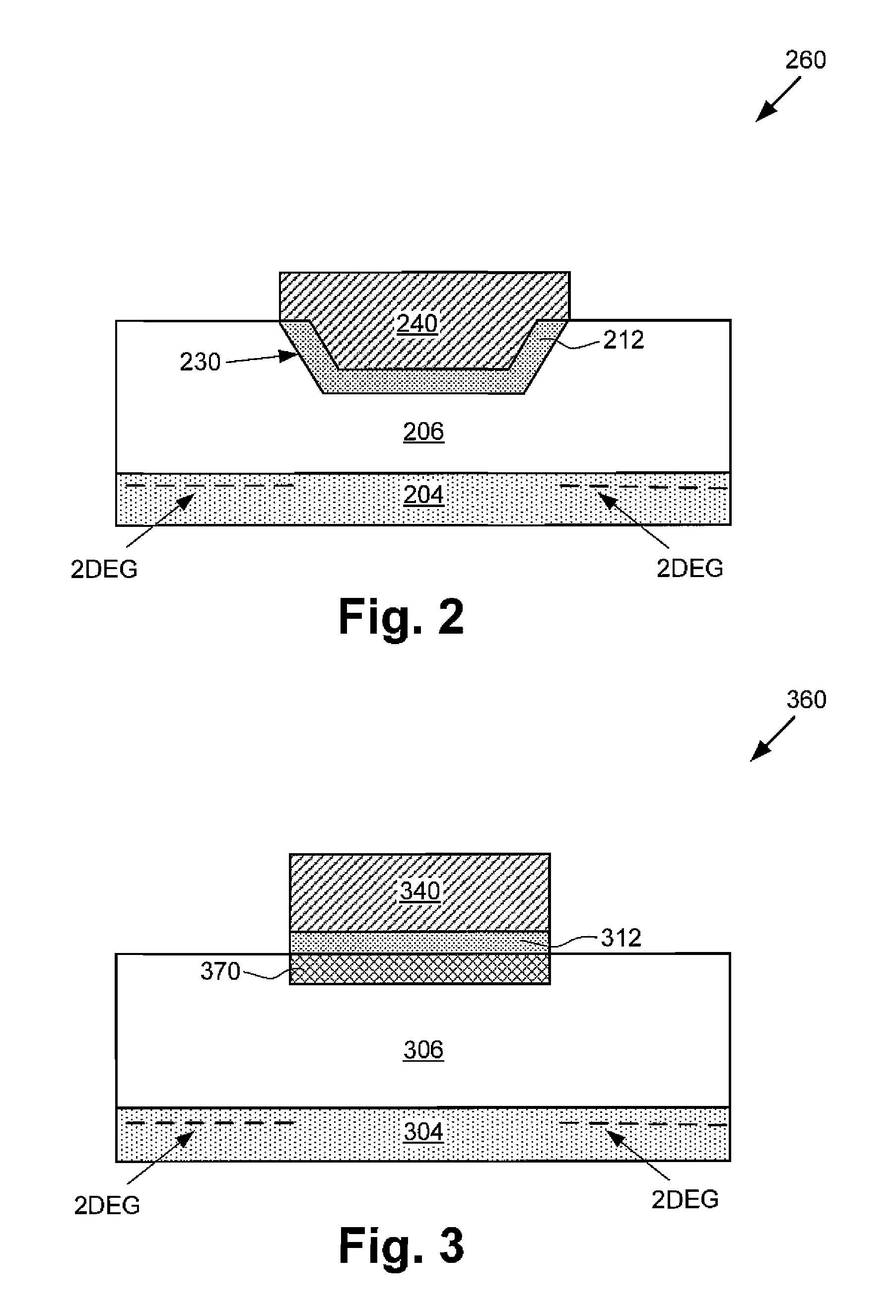
[0014]The present invention is directed to III-nitride devices, particularly enhancement mode III-nitride devices, including modification to alter formation of 2DEG (two dimensional electron gas). Modifications based on aluminum introduction, for example by doping or other methods, are of notable interest in the present invention. The following description contains specific information pertaining to the implementation of the present invention. One skilled in the art will recognize that the present invention may be implemented in a manner different from that specifically discussed in the present application. Moreover, some of the specific details of the invention are not discussed in order not to obscure the invention.

[0015]The drawings in the present application and their accompanying detailed description are directed to merely exemplary embodiments of the invention. To maintain brevity, other embodiments of the present invention are not specifically described in the present applica...


PUM


Abstract

Disclosed is a III-nitride heterojunction device that includes a conduction channel having a two dimensional electron gas formed at an interface between a first III-nitride material and a second III-nitride material. A modification including a contact insulator, for example, a gate insulator formed under a gate contact, is disposed over the conduction channel, wherein the contact insulator includes aluminum to alter formation of the two dimensional electron gas at the interface. The contact insulator can include AlSiN, or can be SiN doped with aluminum. The modification results in programming the threshold voltage of the III-nitride heterojunction device to, for example, make the device an enhancement mode device. The modification can further include a recess, an ion implanted region, a diffused region, an oxidation region, and/or a nitridation region. In one embodiment, the first III-nitride material comprises GaN and the second III-nitride material comprises AlGaN.

Description

[0001]The present application claims the benefit of and priority to a pending provisional application entitled “Programmable III-Nitride Transistor with Aluminum-Doped Gate,” Ser. No. 61 / 340,802 filed on Mar. 22, 2010. The disclosure in that pending provisional application is hereby incorporated fully by reference into the present application.BACKGROUND OF THE INVENTION[0002]In the present application, “group III-V semiconductor” or the like refers to a compound semiconductor that includes at least one group III element and at least one group V element, such as, but not limited to, gallium nitride (GaN), gallium arsenide (GaAs), aluminum gallium arsenide (AlGaAs), indium gallium nitride (InGaN) and the like. Analogously, “III-nitride semiconductor” or the like refers to a compound semiconductor that includes nitrogen and at least one group III element, such as, but not limited to, GaN, AlGaN, InN, AlN, InGaN, InAlGaN and the like.[0003]1. Field of the Invention[0004]The present inve...

Claims


Application Information

Patent Timeline
IPC IPC(8): H01L29/778H01L29/20
CPCH01L29/2003H01L29/207H01L29/803H01L29/4232H01L29/7787H01L29/42316
Inventor BRIERE, MICHAEL A.
Owner INFINEON TECH AMERICAS CORP
Why Eureka
Try Eureka