Optical signal processing device

Active Publication Date: 2011-09-22
NIPPON TELEGRAPH & TELEPHONE CORP
View PDF5 Cites 7 Cited by
  • Summary
  • Abstract
  • Description
  • Claims
  • Application Information

AI Technical Summary

Benefits of technology

[0018]As described above, in the conventional optical signal processing device, a confocal optical system is configured in which the focusing lens is positioned at the substantial intermediate point of the free space optical path. This has caused a disadvantage of a long distance of the space optical system. Furthermore, a disadvantage also has bee caused where a high accuracy is required in the adjustment process during the manufacture of the optical signal processing device. Furthermore, a disadvantage also has bee caused where the device and manufacture method require a high cost. The present invention solves the above-described disadvantages, shortens the free space optical system of the optical signal processing device, and simplifies the adjustment of the optical signal processing device.
[0028]As described above, according to the present invention, the length of the free space optical system of the optical signal processing device can be reduced to about a half of the conventional one. Furthermore, the optical signal processing device can be adjusted easily.

Problems solved by technology

However, the conventional optical signal processing device had a disadvantage in that a long optical path of a free space optical system prevents the entire device from having a smaller size.

Method used


Image

  • Optical signal processing device
  • Optical signal processing device
  • Optical signal processing device

Examples


embodiment 1

Illustrative Embodiment 1

[0052]FIG. 3A illustrates a configuration of more specific Illustrative Embodiment 1 of the optical signal processing device of the present invention realized by AWG. In illustrative Embodiment 1, the spectroscopic element 10 having the focusing power in FIG. 2 is configured by the AWG 11 having a focusing power. The AWG is characterized in having a smaller size when compared to other spectroscopic elements such as a grating and a prism. Thus, by applying the AWG to the shortened optical system of the present invention, the entire optical signal processing device can have a smaller size. Furthermore, since the AWG can include a focusing power by merely changing the waveguide pattern, an additional manufacture process required in the case of other spectroscopic elements is not required.

[0053]As shown in FIG. 3A, the AWG 11 having a focusing power includes the arrayed-waveguide 15 having a focusing power, an input waveguide 13, and the slab waveguide 14. From ...

embodiment 2

Illustrative Embodiment 2

[0056]FIG. 4A illustrates a configuration of Illustrative Embodiment 2 of the optical signal processing device of the present invention using the AWG. In Illustrative Embodiment 1 shown in FIG. 3A, the AWG 11 had a focusing power only in the x axis direction and no lens power was provided in a direction vertical to the AWG substrate. Thus, the focusing lens 2 can be provided as a cylindrical lens having a focusing power only in the x axis direction and other focusing lenses having a focusing power in a direction vertical to the substrate can be additionally provided.

[0057]As shown in FIG. 4A, Illustrative Embodiment 2 is characterized in that the focusing lens 2 is substituted with an x-cylindrical lens 7 having a focusing power in the x axis direction and a y-cylindrical lens 8 having a focusing power in the y axis direction is additionally provided at the center of the optical path. A difference from the optical signal processing device of the configuratio...

embodiment 3

Illustrative Embodiment 3

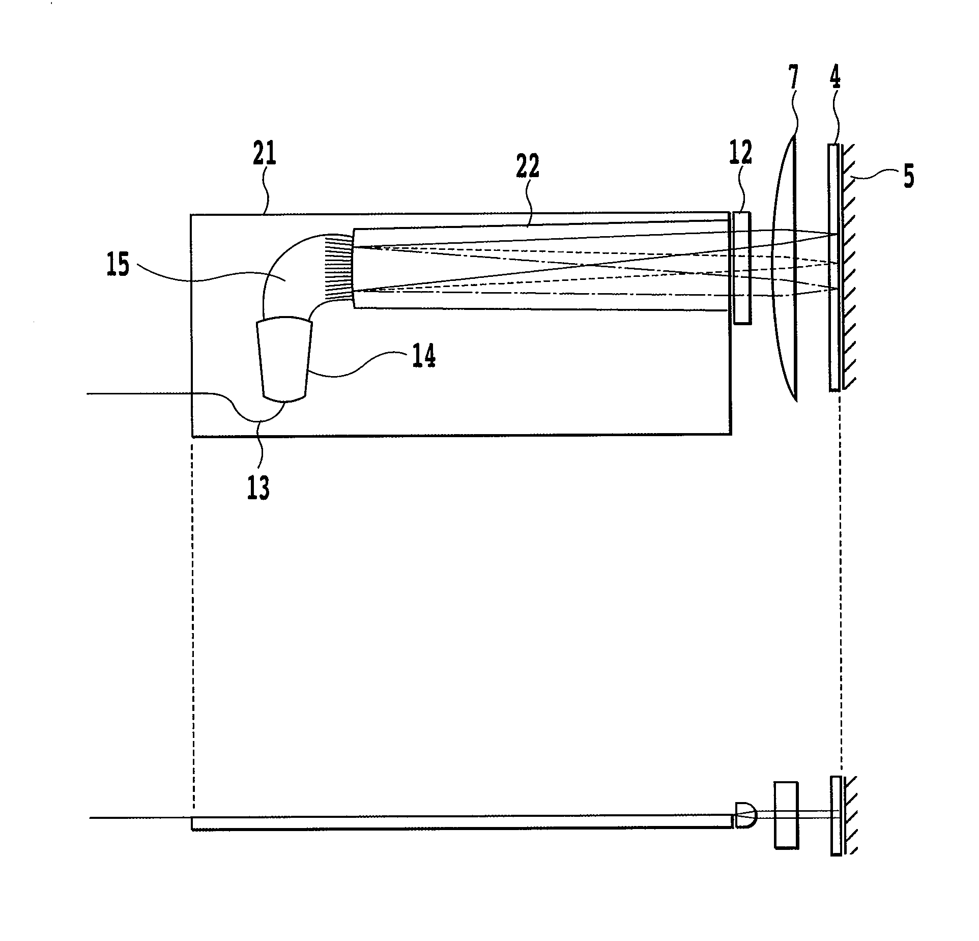
[0062]FIG. 5 illustrates a configuration of Illustrative Embodiment 3 of the optical signal processing device of the present invention using the AWG. Illustrative Embodiment 3 is characterized in that a part of the free space optical system in Illustrative Embodiment 2 is further incorporated in the AWG having a focusing power to thereby further reduce the length of the free space optical system. Specifically, the AWG 21 having a focusing power includes the input waveguide 13, the slab waveguide 14, and the arrayed-waveguide 15 having a focusing power and further includes an output slab waveguide 22. Based on the optical coupling conditions, the front focal point position of the x-cylindrical lens 7 must optically correspond to the dispersion center of the AWG 21 (i.e., a position at the boundary between the arrayed-waveguide 15 and the slab waveguide 22). The expression “optically correspond” means that an optical reduced length obtained by dividing an real...


PUM


Abstract

In a conventional optical signal processing device, a confocal optical system is configured in which a focusing lens is positioned at a substantially-intermediate point of a free space optical path. Thus, the free space optical system had a long length. It has been difficult to reduce the size of the entire device. The optical signal processing device of the present invention uses a lens layout configuration different from the confocal optical system to thereby significantly reduce the length of the system. The optical signal processing device consists of the first focusing lens positioned in the close vicinity of a signal processing device, and the second focusing lens positioned in the vicinity of a dispersing element. A distance between the dispersing element and the signal processing device is approximately a focal length of the first focusing lens. Compared with the conventional technique, the length of the optical path can be halved.

Description

TECHNICAL FIELD[0001]The present invention relate to an optical signal processing device. In particular, the present invention relates to an optical signal processing circuit including a lens.BACKGROUND ART[0002]With the advance of an optical communication network having a high speed and a high capacity, needs for an optical signal processing device, a typical example of which is the wavelength division multiplexing (WDM) transmission signal processing, also has been increased. For example, a function has been required to switching a path of a multiplexed optical signal among nodes. By directly subjecting an optical signal to a path conversion without using an optical-electrical conversion, more optical signal processing devices having a higher speed have been made.[0003]On the other hand, from a viewpoint of an optical signal processing device having a smaller size and integration, a planar lightwave circuit (PLC) has been researched and developed. In the PLC, a core made of silica...

Claims


Application Information

Patent Timeline
IPC IPC(8): G02F1/01G02F1/29
CPCG02B6/12021G02F1/2955G02B6/356G02B6/12033
Inventor OOBA, NAOKISUZUKI, KENYAISHII, MOTOHAYAMINO, SHINJIARATAKE, ATSUSHI
Owner NIPPON TELEGRAPH & TELEPHONE CORP
Why Eureka
Try Eureka