Method of manufacturing magnetoresistive element having a pair of free layers

Active Publication Date: 2011-09-29
TDK CORPARATION
View PDF4 Cites 20 Cited by
  • Summary
  • Abstract
  • Description
  • Claims
  • Application Information

AI Technical Summary

Benefits of technology

[0022]It is an object of the present invention to provide a method of manufacturing a magnetoresistive element that has a pair of free layers coupled to a pair of shields, the method allowing stable magnetic coupling between the upper one of the free layers and the upper one of the shields.
[0032]According to the method of manufacturing the magnetoresistive element of the present invention, in the step of forming the MR stack and the nonmagnetic layer, a protection layer is formed on the top surface of a layered film that is to be patterned into the MR stack later, and then the layered film and the protection layer are etched by using a mask. Subsequently, the nonmagnetic layer is formed with the mask left intact. After the removal of the mask, the protection layer is removed at least by wet etching. Consequently, according to the present invention, it is possible to flatten the top surface of the magnetic cap layer which is the uppermost layer of the MR stack. According to the present invention, it is thus possible to provide stable magnetic coupling between the second free layer which is the upper one of the free layers and the second exchange coupling shield layer which is the upper one of the exchange coupling shield layers.

Problems solved by technology

Disadvantageously, however, this method imposes limitation on the material and thickness of the spacer layer so as to allow antiferromagnetic coupling between the pair of ferromagnetic layers.
In addition, since this method limits the material of the spacer layer to nonmagnetic conductive materials, it is applicable to neither a TMR element which is expected to provide a high output, nor a GMR element of CPP structure of current-confined-path type which is an MR element that is also expected to provide a high output and whose spacer layer includes a portion that allows the passage of currents and a portion that intercepts the passage of currents.
The foregoing method further has the disadvantage that, even if it could be possible to make the directions of magnetization of the pair of ferromagnetic layers antiparallel to each other, it is difficult to make them parallel to the track width direction with reliability.
In the shield-coupling MR element, the magnetic coupling between the second free layer and the second shield is difficult to secure if the MR stack is small in dimension in the track width direction in particular.
As a result, the following problem was found to occur in association with the method.
This consequently makes the magnetic stack unstable both in its shielding capability and its capability of controlling the direction of magnetization of the second free layer.
In such a case, it also becomes difficult to control the average exchange coupling magnetic field in each single MR element, so that characteristic variations among a plurality of MR elements increase.
This makes the foregoing problem even more significant.
Such a method has the problem of high manufacturing cost since the CMP process is needed.
Removing the resist residues by ashing or the like causes the problem that the MR stack becomes uneven in its top surface.

Method used


Image

  • Method of manufacturing magnetoresistive element having a pair of free layers
  • Method of manufacturing magnetoresistive element having a pair of free layers
  • Method of manufacturing magnetoresistive element having a pair of free layers

Examples


modification example

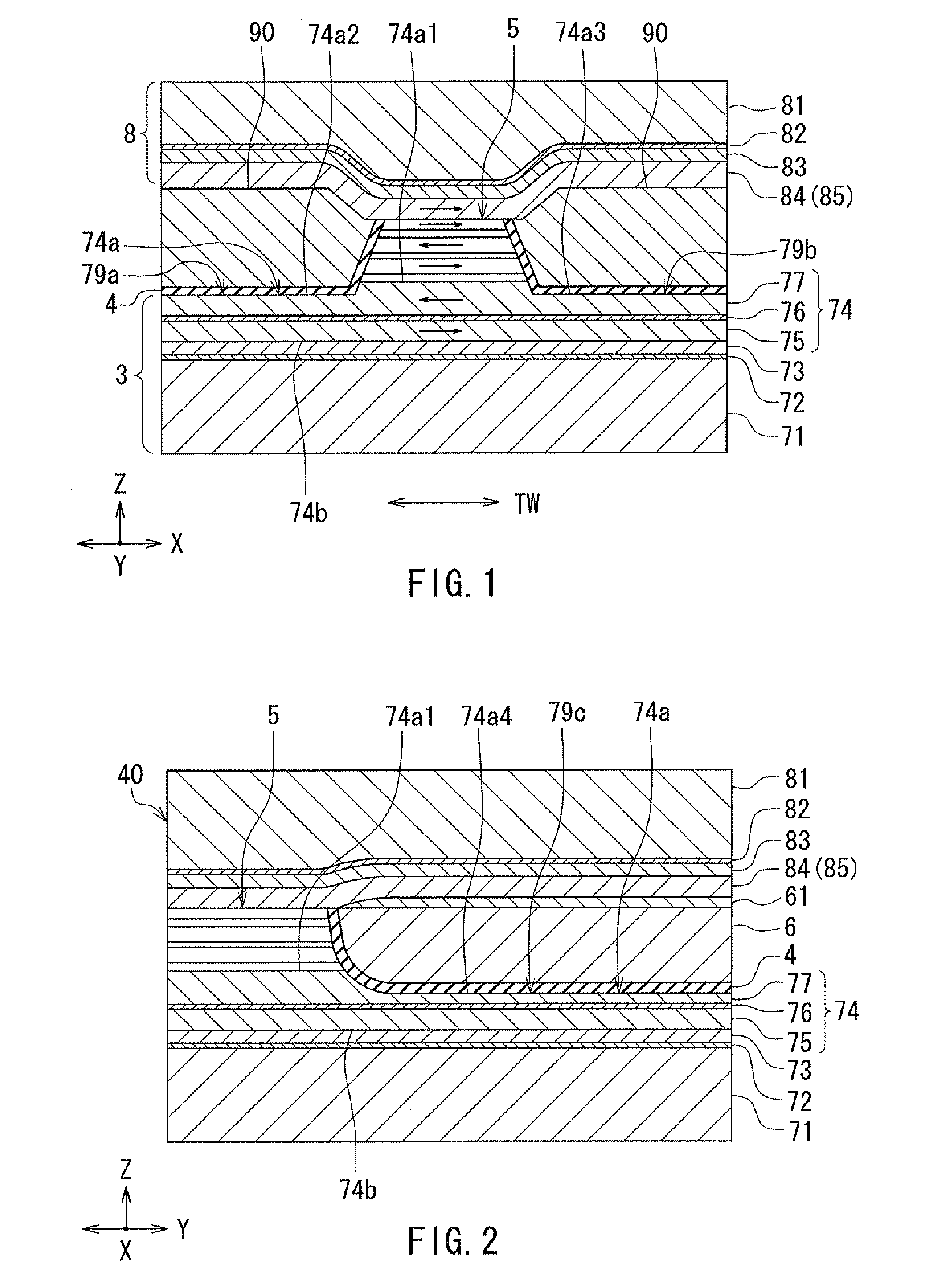
[0181]A modification example of the method of manufacturing the MR element according to the present embodiment will now be described with reference to FIG. 28 and FIG. 29. FIG. 28 and FIG. 29 each show a cross section of a stack of layers in the process of manufacturing the MR element, the cross section being perpendicular to the medium facing surface 40 and the top surface of the substrate 1. The portions lying below the magnetic layer 77P are omitted in FIG. 28 and FIG. 29. The steps of this modification example are the same as those of the method of manufacturing the MR element shown in FIG. 13 to FIG. 16 up to the step of forming the mask 93.

[0182]FIG. 28 and FIG. 29 show the step after the formation of the mask 93. In this step, the layered film 5P and the protection layer 91 are etched into a predetermined shape by ion milling using ion beams in more than one direction of travel. This step will be described in detail below.

[0183]In this step, like the step shown in FIG. 17, th...


PUM

PropertyMeasurementUnit
Adhesion strengthaaaaaaaaaa
Electrical conductoraaaaaaaaaa
Magnetizationaaaaaaaaaa

Abstract

An MR element includes a first exchange coupling shield layer, an MR stack, and a second exchange coupling shield layer that are arranged in this order from the bottom, and a nonmagnetic layer surrounding the MR stack. The MR stack includes a first free layer, a spacer layer, a second free layer, and a magnetic cap layer that are arranged in this order from the bottom. The magnetization direction of the first free layer is controlled by the first exchange coupling shield layer. The second free layer is magnetically coupled to the second exchange coupling shield layer via the magnetic cap layer for magnetization direction control. In the step of forming the MR stack and the nonmagnetic layer, a protection layer is formed on a layered film that will be the MR stack later, and a mask is then formed on the protection layer. Next, the layered film and the protection layer are etched using the mask and then the nonmagnetic layer is formed. After removal of the mask, the protection layer is removed by wet etching.

Description

BACKGROUND OF THE INVENTION[0001]1. Field of the Invention[0002]The present invention relates to a method of manufacturing a magnetoresistive element that is for use in, for example, a thin-film magnetic head, and has a pair of free layers coupled to a pair of shields.[0003]2. Description of the Related Art[0004]Recently, magnetic disk drives have been improved in areal recording density, and thin-film magnetic heads of improved performance have been demanded accordingly. Among the thin-film magnetic heads, a composite thin-film magnetic head has been used widely. The composite thin-film magnetic head has a structure in which a read head including a magnetoresistive element (hereinafter, also referred to as MR element) for reading and a write head including an induction-type electromagnetic transducer for writing are stacked on a substrate.[0005]Examples of MR elements include a giant magnetoresistive (GMR) element utilizing a giant magnetoresistive effect and a tunneling magnetores...

Claims


Application Information

Patent Timeline
IPC IPC(8): G11B5/127
CPCB82Y25/00Y10T29/49046G01R33/093G01R33/098G11B5/3163G11B5/3912G11B5/3945G11B5/398H01F10/3254H01F10/3263H01F10/3272H01F41/308H01L43/12Y10T29/49052Y10T29/49048Y10T29/49032Y10T29/49044Y10T29/49043B82Y40/00H10N50/01
Inventor MIYAUCHI, DAISUKEMACHITA, TAKAHIKOKAWAMORI, KEITA
Owner TDK CORPARATION
Why Eureka
Try Eureka