Light-Emitting Element, Light-Emitting Device, Electronic Device, and Lighting Device
a technology of light-emitting elements and electronic devices, which is applied in the direction of static indicating devices, instruments, other domestic objects, etc., can solve the problems of light-emitting elements and reduce driving voltage, and achieve the effects of preventing the formation of pn junctions, reducing driving voltage, and reducing driving voltag
- Summary
- Abstract
- Description
- Claims
- Application Information
AI Technical Summary
Benefits of technology
Problems solved by technology
Method used
Image

Examples
embodiment 1
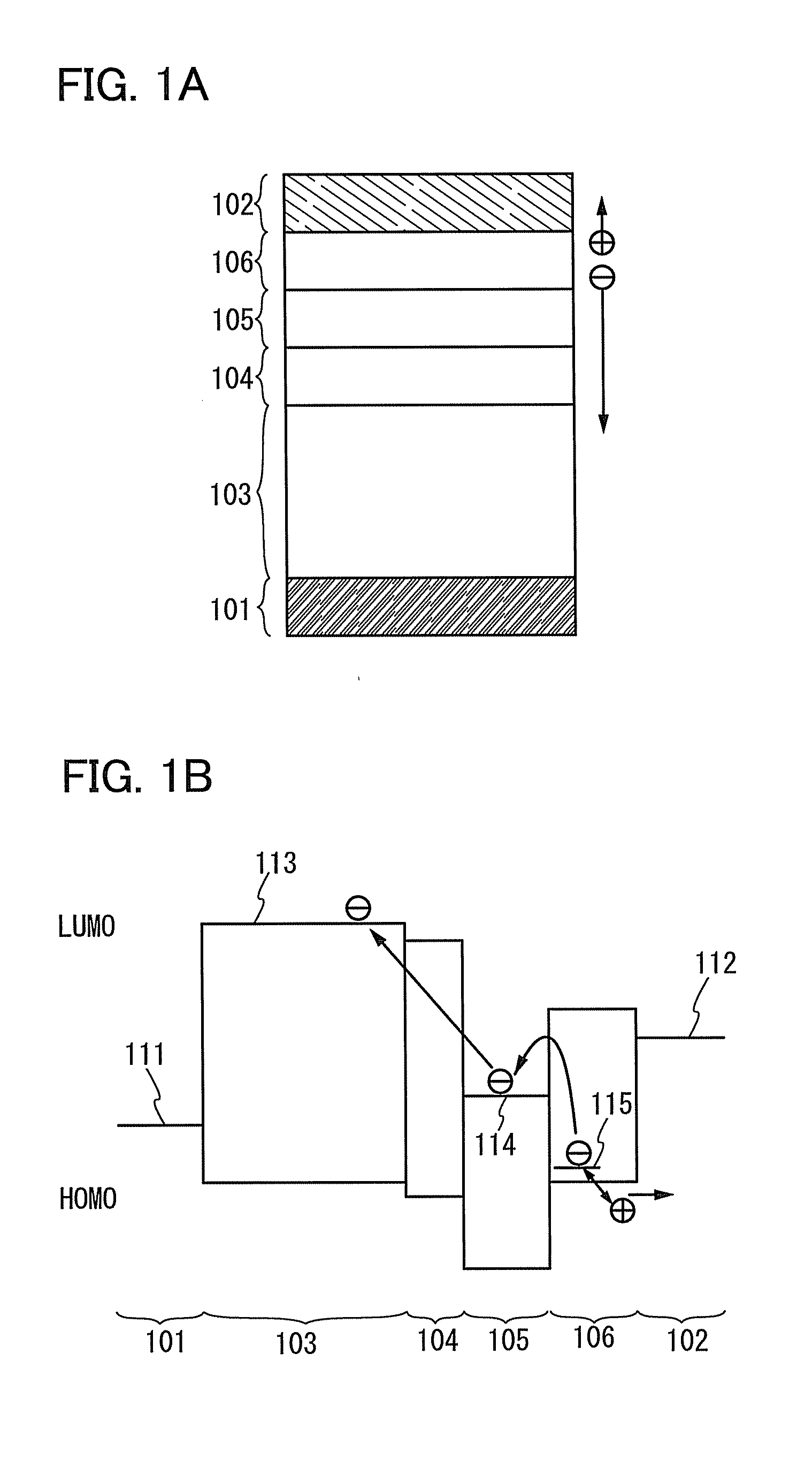
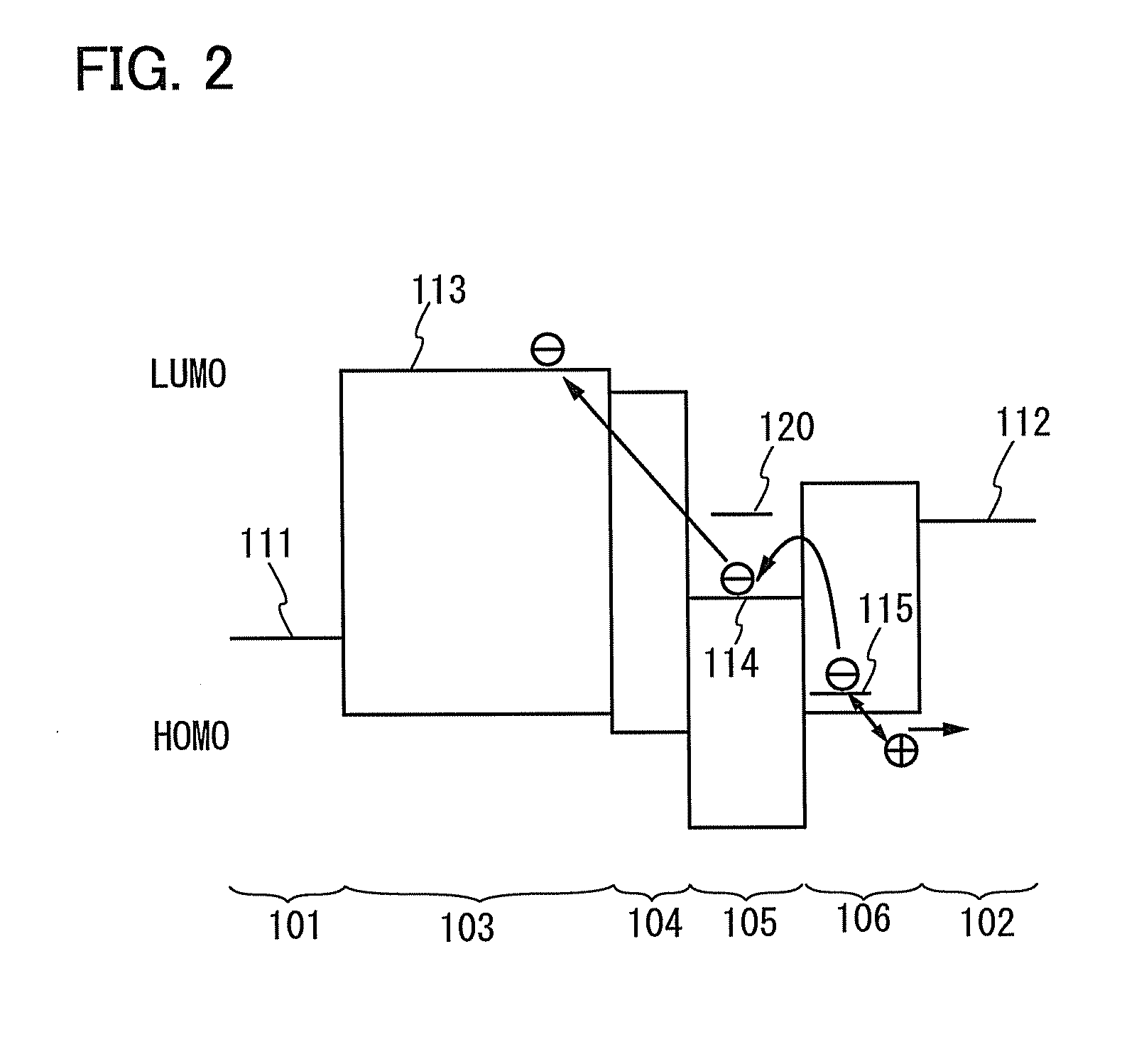
[0059]An element structure of a light-emitting element which is one embodiment of the present invention will be described with reference to FIGS. 1A and 1B and FIG. 2.
[0060]The light-emitting element illustrated in FIG. 1A has an EL layer 103 including a light-emitting region between a pair of electrodes (an anode 101 and a cathode 102). Between the cathode 102 and the EL layer 103, the element has a first layer 106, a second layer 105, and a third layer 104 in order from the cathode 102 side.
[0061]The first layer 106 is between the cathode 102 and the second layer 105, and in contact with the cathode 102 and with the second layer 105. The first layer 106 includes a substance having a hole-transport property and an acceptor substance with respect to the substance having a hole-transport property and serves as a charge generation region. Holes and electrons are considered to be generated in such a manner that the substance having a hole-transport property and the acceptor substance f...
embodiment 2
[0118]In this embodiment, an example of the light-emitting element described in Embodiment 1 will be described with reference to FIGS. 3A and 3B.
[0119]As illustrated in FIG. 3A, in the light-emitting element, the EL layer 103 including a light-emitting region is interposed between the pair of electrodes (the anode 101 and the cathode 102). Between the cathode 102 and the EL layer 103, the first layer 106 serving as a charge generation region, the second layer 105 serving as an electron-relay layer, and the third layer 104 serving as an electron-injection buffer are sequentially stacked over the cathode 102.
[0120]The same materials as described in Embodiment 1 can be used for the anode 101, the cathode 102, the EL layer 103, the first layer 106, and the second layer 105.
[0121]As a substance used for the third layer 104, the following substances having a high electron-injection property can be given as examples: alkali metals such as lithium (Li) and cesium (Cs), alkaline-earth metals...
embodiment 3
[0129]In this embodiment, an example of the light-emitting element described in Embodiment 1 will be described with reference to FIGS. 4A and 4B.
[0130]As illustrated in FIG. 4A, in the light-emitting element, the EL layer 103 including a light-emitting region is interposed between the pair of electrodes (the anode 101 and the cathode 102). Between the cathode 102 and the EL layer 103, the first layer 106 serving as a charge generation region, the second layer 105 serving as an electron-relay layer, and the third layer 104 serving as an electron-injection buffer are sequentially stacked over the cathode 102. The third layer 104 includes the substance having an electron-transport property and the donor substance.
[0131]In the third layer 104, the donor substance is preferably added so that the mass ratio thereof to the substance having an electron-transport property is greater than or equal to 0.001:1 and less than or equal to 0.1:1. Accordingly, the function as an electron-injection b...
PUM
 Abstract
Description
Claims
Application Information
 - R&D
- Intellectual Property
- Life Sciences
- Materials
- Tech Scout
- Unparalleled Data Quality
- Higher Quality Content
- 60% Fewer Hallucinations
Browse by: Latest US Patents, China's latest patents, Technical Efficacy Thesaurus, Application Domain, Technology Topic, Popular Technical Reports.
© 2025 PatSnap. All rights reserved.Legal|Privacy policy|Modern Slavery Act Transparency Statement|Sitemap|About US| Contact US: help@patsnap.com