Semiconductor light-emitting device and manufacturing method

a technology of semiconductor light-emitting device and manufacturing method, which is applied in the direction of discharge tube luminescnet screen, lighting and heating apparatus, transportation and packaging, etc., can solve the problems of difficult for the semiconductor light-emitting device and difficult for the conventional semiconductor light-emitting devi

Active Publication Date: 2011-09-29
STANLEY ELECTRIC CO LTD
View PDF4 Cites 36 Cited by
  • Summary
  • Abstract
  • Description
  • Claims
  • Application Information

AI Technical Summary

Benefits of technology

[0035]According to the exemplary manufacturing method described above for the semiconductor light-emitting devices, the transparent plate can be attached on the wavelength converting layer using its own weight by placing it on the transparent adhesive layer. The wavelength converting layer and the diffusing reflection member can be solidified by a similar method as compared to conventional processes. Thus, the method can provide reliable semiconductor light-emitting devices used for a vehicle headlight using manufacturing machines that are similar to those used to manufacture conventional semiconductor light-emitting devices.

Problems solved by technology

However, it may be difficult for the semiconductor light-emitting device 60 to provide the side surface 53 of the wavelength converting layer 52 on the same surface as the boundary 55 between the wavelength converting layer 52 and the reflecting member 54 as shown in FIG. 9.
Thus, it may be difficult for the conventional semiconductor light-emitting device 60 to provide a favorable horizontal cut-off line for a low beam.

Method used


Image

  • Semiconductor light-emitting device and manufacturing method
  • Semiconductor light-emitting device and manufacturing method
  • Semiconductor light-emitting device and manufacturing method

Examples


Embodiment Construction

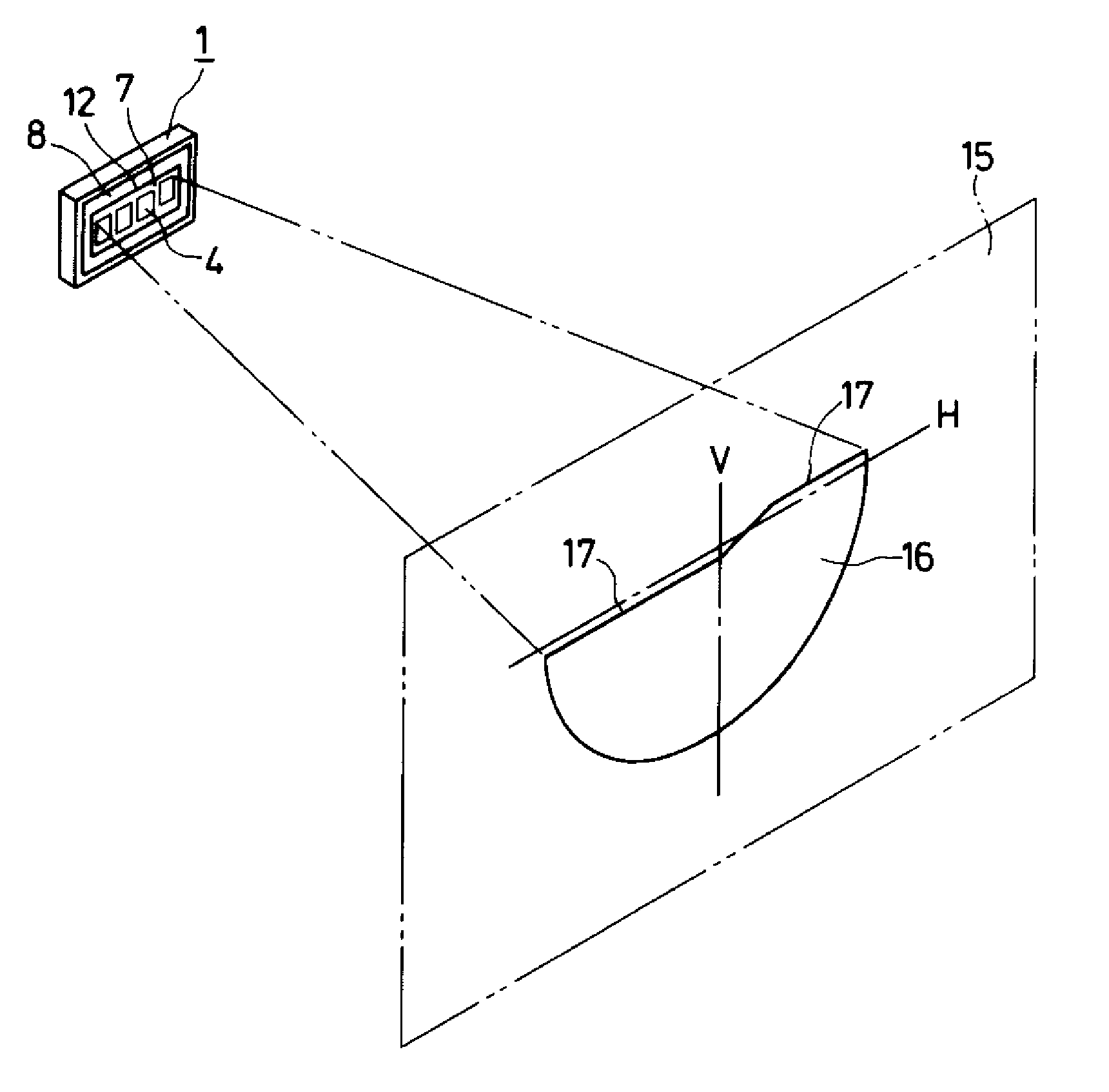
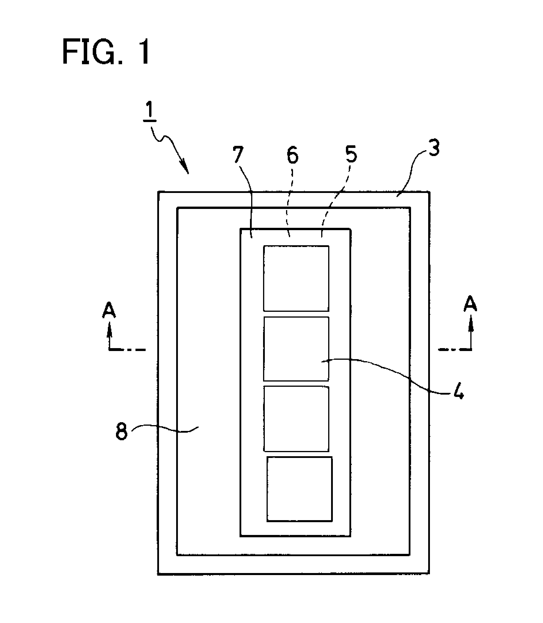
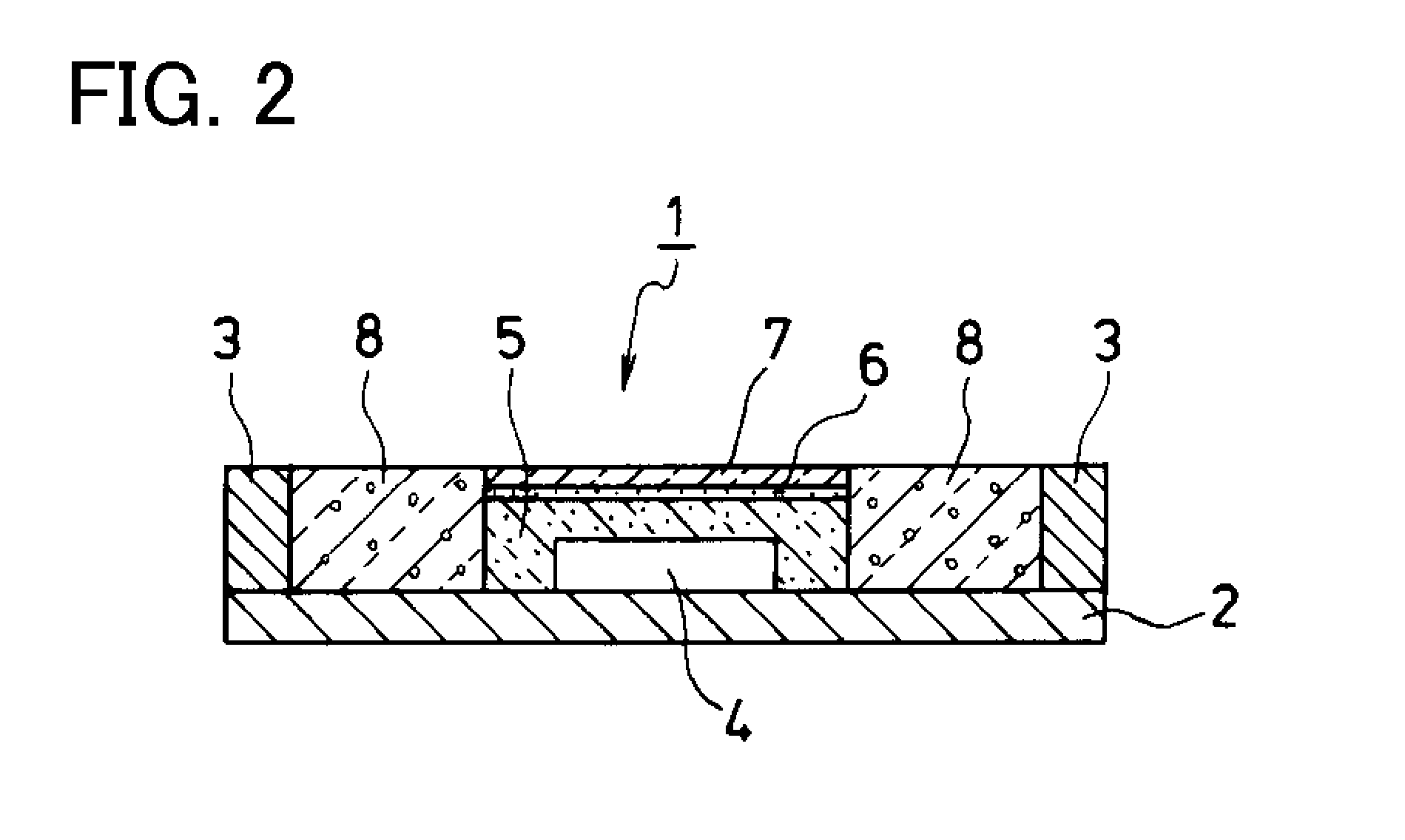
[0047]Exemplary embodiments and manufacturing methods of the disclosed subject matter will now be described in detail with reference to FIGS. 1 to 7. FIG. 1 is a top view showing an exemplary embodiment of a semiconductor light-emitting device made in accordance with principles of the disclosed subject matter. FIG. 2 is a cross-section view depicting the semiconductor light-emitting device taken along line A-A shown in FIG. 1, and FIG. 3 is a partial close-up view of the semiconductor light-emitting device of FIG. 2.

[0048]The semiconductor light-emitting device 1 can include: a base board 2 having a mounting surface and conductor patterns formed on the mounting surface; at least one semiconductor light-emitting chip 4 having chip electrodes mounted on the mounting surface of the base board 2, and each of the chip electrodes electrically connected to respective conductor patterns of the base board 2; a wavelength converting layer 5 formed around the semiconductor light-emitting chip ...


PUM

PropertyMeasurementUnit
thicknessaaaaaaaaaa
peak wavelengthaaaaaaaaaa
color temperatureaaaaaaaaaa

Abstract

A semiconductor light-emitting device and a method for manufacturing the same can include a wavelength converting layer encapsulating at least one semiconductor light-emitting chip in order to emit various colored lights including white light. The semiconductor light-emitting device can include a base board, a frame located on the base board, the chip mounted on the base board, the wavelength converting layer formed around the chip, a transparent plate located on the wavelength converting layer and a diffusing reflection member disposed between the frame and both side surfaces of the wavelength converting layer and the transparent plate. The device can be configured to improve the linearity of a boundary between the diffusing reflection member and both side surfaces by using the transparent plate, and therefore can be used for a headlight that can form a favorable horizontal cut-off line corresponding to the boundary via a projector lens without a shade.

Description

[0001]This application claims the priority benefit under 35 U.S.C. §119 of Japanese Patent Application No. 2010-068088 filed on Mar. 24, 2010, which is hereby incorporated in its entirety by reference.BACKGROUND[0002]1. Field[0003]The presently disclosed subject matter relates to semiconductor light-emitting devices including a semiconductor light-emitting chip and to manufacturing methods for the same, and more particularly, to semiconductor light-emitting devices for a vehicle light, for example a headlight, that can provide a favorable horizontal cut-off line for a low beam without a shade, and to methods of manufacturing such devices.[0004]2. Description of the Related Art[0005]Semiconductor light-emitting devices that include an LED chip have been used for vehicle headlights in recent years. Vehicle headlights can be classified into two major groups, a reflector type and a projector type. A conventional LED light source using a plurality of LED chips and a vehicle lamp using th...

Claims


Application Information

Patent Timeline
Patent Type & Authority Applications(United States)
IPC IPC(8): F21V9/00F21V11/00H01L21/00
CPCH01L33/50H01L25/0753F21S48/1154H01L2924/0002H01L33/58Y10T29/41H01L2924/00F21S41/151
Inventor SEKO, TOSHIHIRO
Owner STANLEY ELECTRIC CO LTD
Why Eureka
Try Eureka