Channel chip and jig

Inactive Publication Date: 2011-09-29
ORMON CORP
View PDF3 Cites 35 Cited by
  • Summary
  • Abstract
  • Description
  • Claims
  • Application Information

AI Technical Summary

Benefits of technology

[0035]According to the present invention, the flat face of the cover is in contact with the film, and accordingly, deformation of the film due to an increase in pressure of the fluid flowing in the channel can be restrained. Thus, the va

Problems solved by technology

Furthermore, since the heating process becomes unnecessary, other processes s

Method used


Image

  • Channel chip and jig
  • Channel chip and jig
  • Channel chip and jig

Examples


Example

First Embodiment

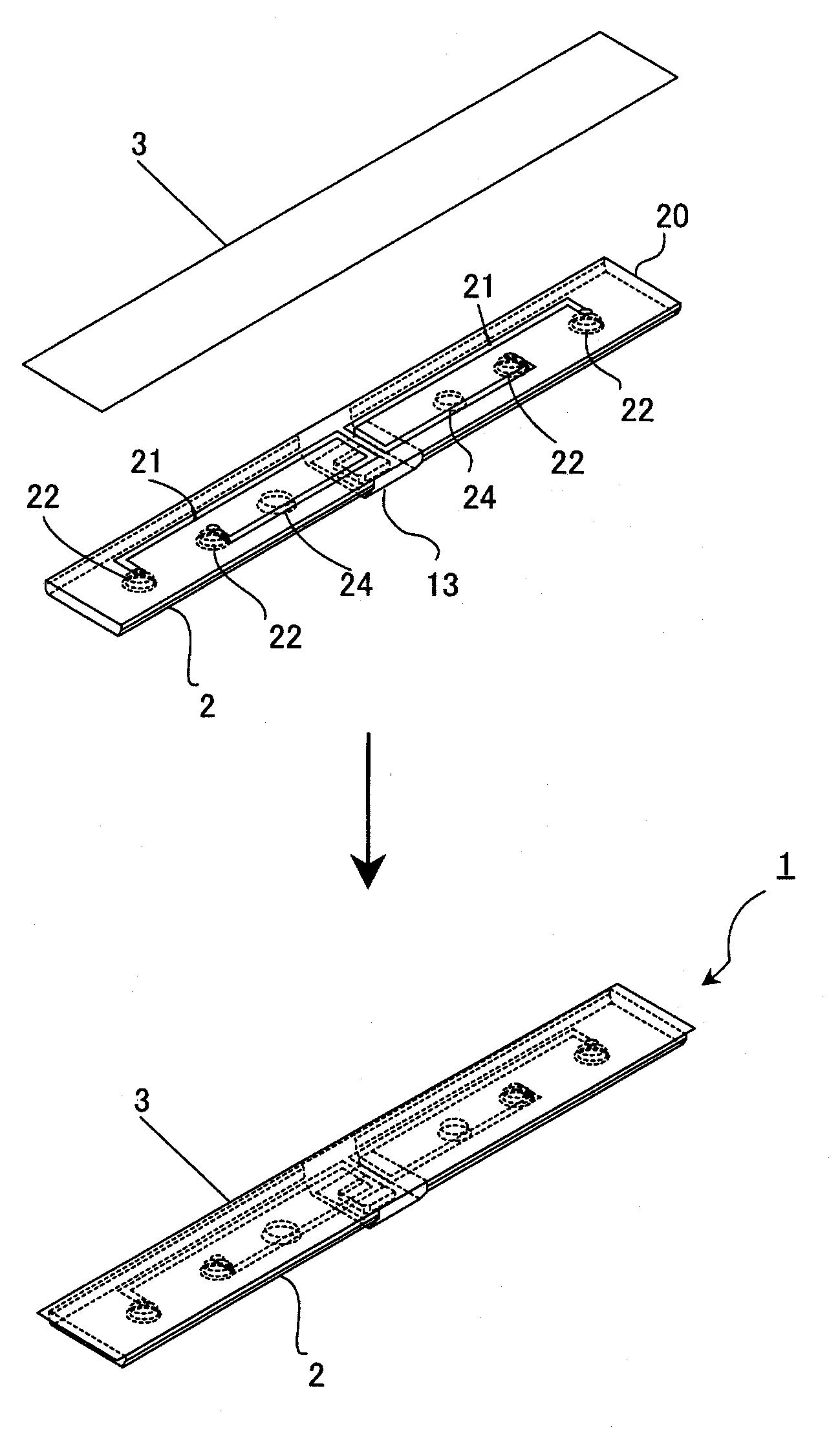
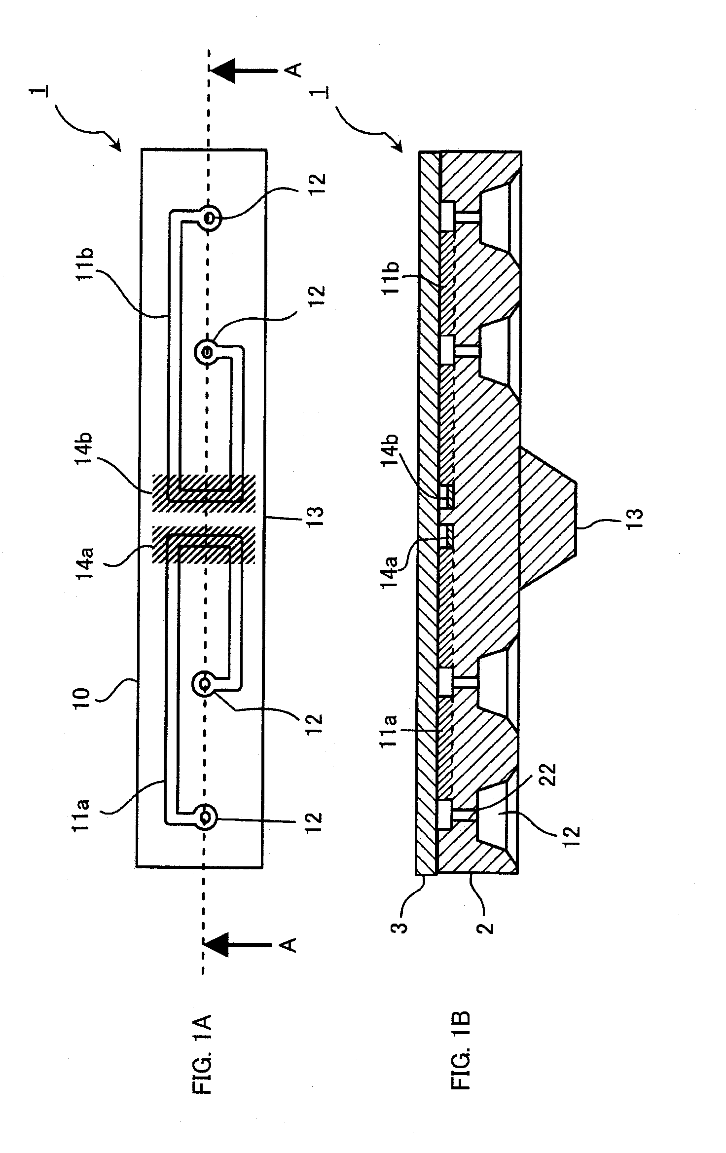
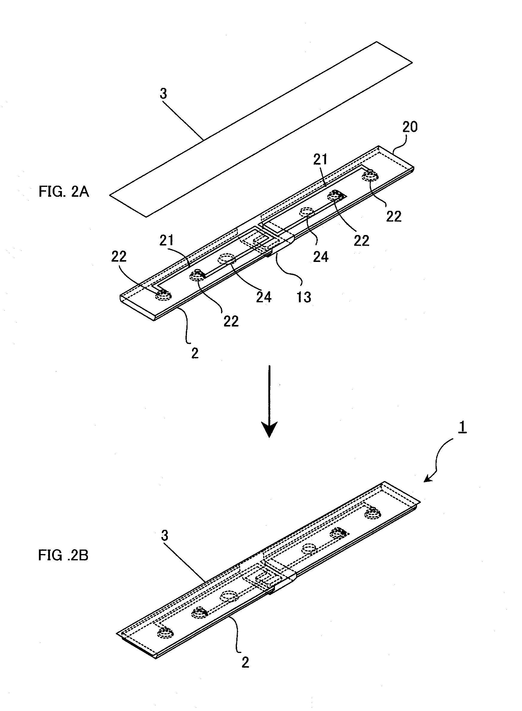
[0068]Referring now to FIGS. 1A through 2B, a channel chip according to a first embodiment of the present invention is described. FIGS. 1A and 1B are schematic views of the channel chip according to this embodiment. FIG. 1A is a schematic plan view of the channel chip, and FIG. 1B is a cross-sectional view of the channel chip, taken along the line A-A of FIG. 1A. FIGS. 2A and 2B are schematic perspective views of the channel chip according to this embodiment. FIG. 2A illustrates a situation where a substrate and a film are separated from each other, and FIG. 2B illustrates a situation where the film is bonded to the substrate.

[0069]In this embodiment described below, an examplary case where a channel chip according to an embodiment of the present invention is used as a sensor chip of a so-called surface plasmon resonance sensor is described. However, the channel chip according to the present invention may be used in other structures.

[0070]As shown in FIGS. 1A and 1B,...

Example

Second Embodiment

[0162]Referring now to FIGS. 26 through 28, a channel chip according to a second embodiment of the present invention is described. FIG. 26 is a graph showing the relationship between a flow rate variation and a signal variation in a channel chip according to the first embodiment. FIG. 27 is a schematic cross-sectional view of the channel chip according to the second embodiment. FIG. 28 is a graph showing the relationship between a flow rate variation and a signal variation in the channel chip according to the second embodiment. The same aspects as those of the first embodiment are not repeated herein, and only the different aspects from the first embodiment are described.

[0163]As shown in FIG. 26, where the flow rate greatly varies, displacement of the film 3 might not be sufficiently restrained simply by placing the flat substrate on the outer face of the film 3 as in the first embodiment. Particularly, in a case where the flow rate varies from a high flow rate to ...


PUM

PropertyMeasurementUnit
Pressureaaaaaaaaaa
Flow rateaaaaaaaaaa
Diameteraaaaaaaaaa

Abstract

A channel chip includes a substrate made of a material capable of transmitting light. The substrate includes a groove to form a channel for allowing a fluid to flow. A film is made of a material capable of transmitting light. The film is bonded to the substrate with a pressure sensitive adhesive agent to seal the groove.

Description

BACKGROUND OF THE INVENTION[0001]1. Field of the Invention[0002]One or more embodiments of the present invention generally relates to a channel chip and, more particularly, to a microchannel chip comprising at least one microchannel, as well as to a jig for holding the channel chip.[0003]2. Description of the Related Art[0004]Microchannel chips are known as chemical analysis chips that are manufactured by using a microelectromechanical system or the like. Various kinds of functions can be integrated on one chip, and specimen materials can be detected with high precision. Accordingly, microchannel chips are used in a wide variety of fields, such as medical industries, environmental industries, food industries, and micro chemical synthesis (Japanese Patent Application Laid-Open Nos. 2008-76208 and 2008-175795, for example). As reaction detecting methods using microchannel chips, known methods are a method that utilizes fluorescent molecules, an absorbance measurement method, an electr...

Claims


Application Information

Patent Timeline
IPC IPC(8): G01N21/75B01L9/00
CPCB01L3/502707B01L3/502715B01L9/527B01L2200/027B01L2200/0689B29C65/4845B01L2300/0816B01L2300/0887B29C66/53461B29L2031/756B29C65/4825B01L2300/0654
Inventor HASUI, RYOSUKEIWASAKA, HIROYUKINISHIKAWA, TAKEOYAMADA, KEISUKEKAMIYAMA, SUSUMU
Owner ORMON CORP
Why Eureka
Try Eureka