Signal shielding through-substrate vias for 3D integration

a technology of through-substrate vias and signals, applied in the direction of semiconductor devices, semiconductor/solid-state device details, electrical apparatus, etc., can solve the problems of limiting the maximum frequency of signals that can be transmitted through the tsv, false transient signals, and imposing limitations on the benefits of 3d integration

Inactive Publication Date: 2011-10-06
GLOBALFOUNDRIES INC
View PDF10 Cites 81 Cited by
  • Summary
  • Abstract
  • Description
  • Claims
  • Application Information

AI Technical Summary

Problems solved by technology

One of the limitations to the benefits of 3D integration is imposed by cross-talk between signals in TSVs.
Cross-talk between TSVs can degrade the overall system level performance of a stacked structure of multiple semiconductor chips by introducing noise into signals through TSVs, which can cause false transient signals and limit the maximum frequency of signals that can be transmitted through the TSVs.

Method used


Image

  • Signal shielding through-substrate vias for 3D integration
  • Signal shielding through-substrate vias for 3D integration
  • Signal shielding through-substrate vias for 3D integration

Examples


first embodiment

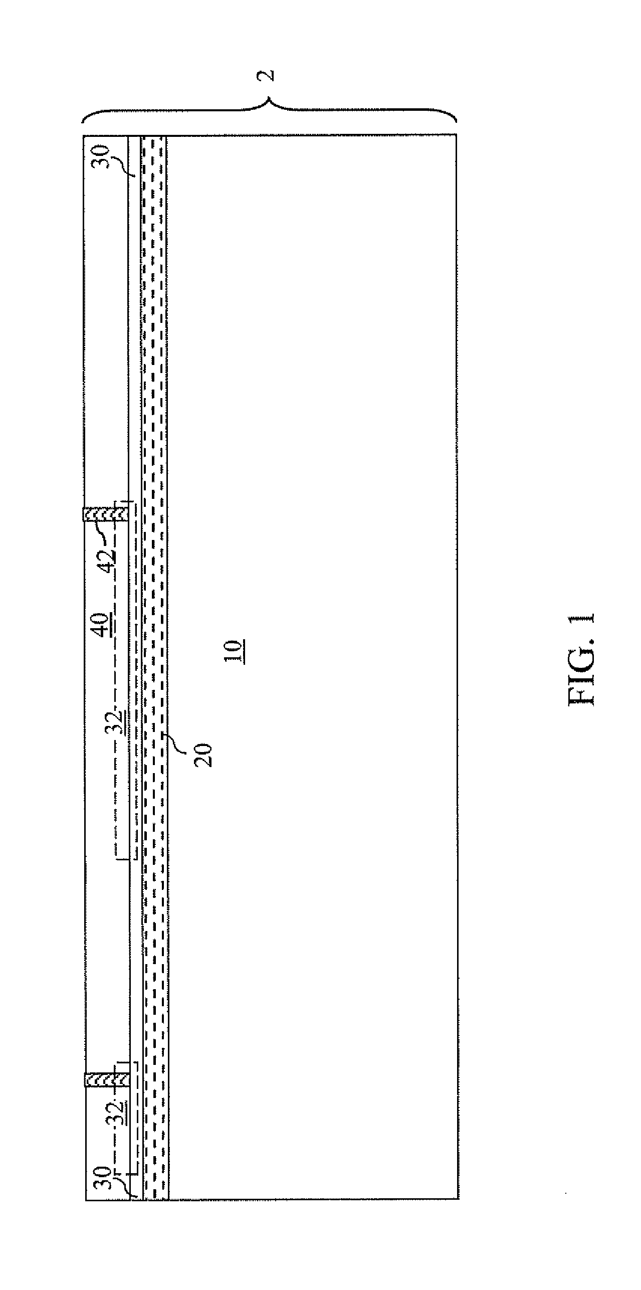
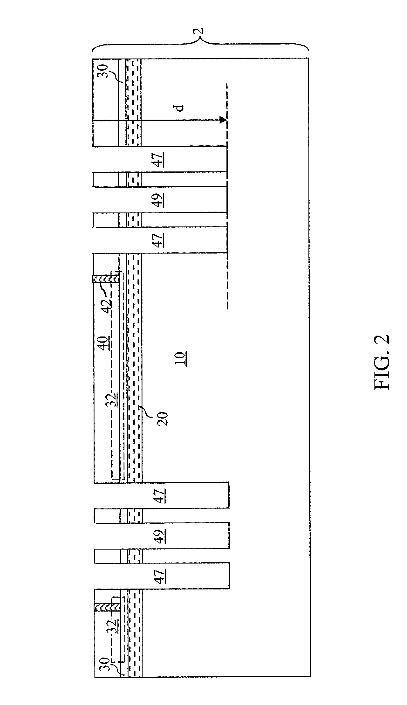
[0023]Referring to FIG. 1, a first exemplary semiconductor structure according to the present invention includes a first substrate 2. The first substrate 2 can include a semiconductor-on-insulator (SOI) substrate, a bulk semiconductor substrate, or a hybrid substrate including at least one SOI portion and at least one bulk portion. If the first substrate 2 includes an SOI substrate, the SOI substrate can contain, from bottom to top, a first handle substrate 10, a first buried insulator layer 20, and a first top semiconductor layer 30. Typical materials employed for the first handle substrate 10 include a semiconductor material or silicate glass.

[0024]The first handle substrate 10 can include a semiconductor material, a dielectric material, a conductive material, or a combination thereof. Typically, the first handle substrate 20 includes a semiconductor material. The thickness of the handle substrate 10 can be from 100 microns to 1,000 microns, although lesser and greater thicknesses...

second embodiment

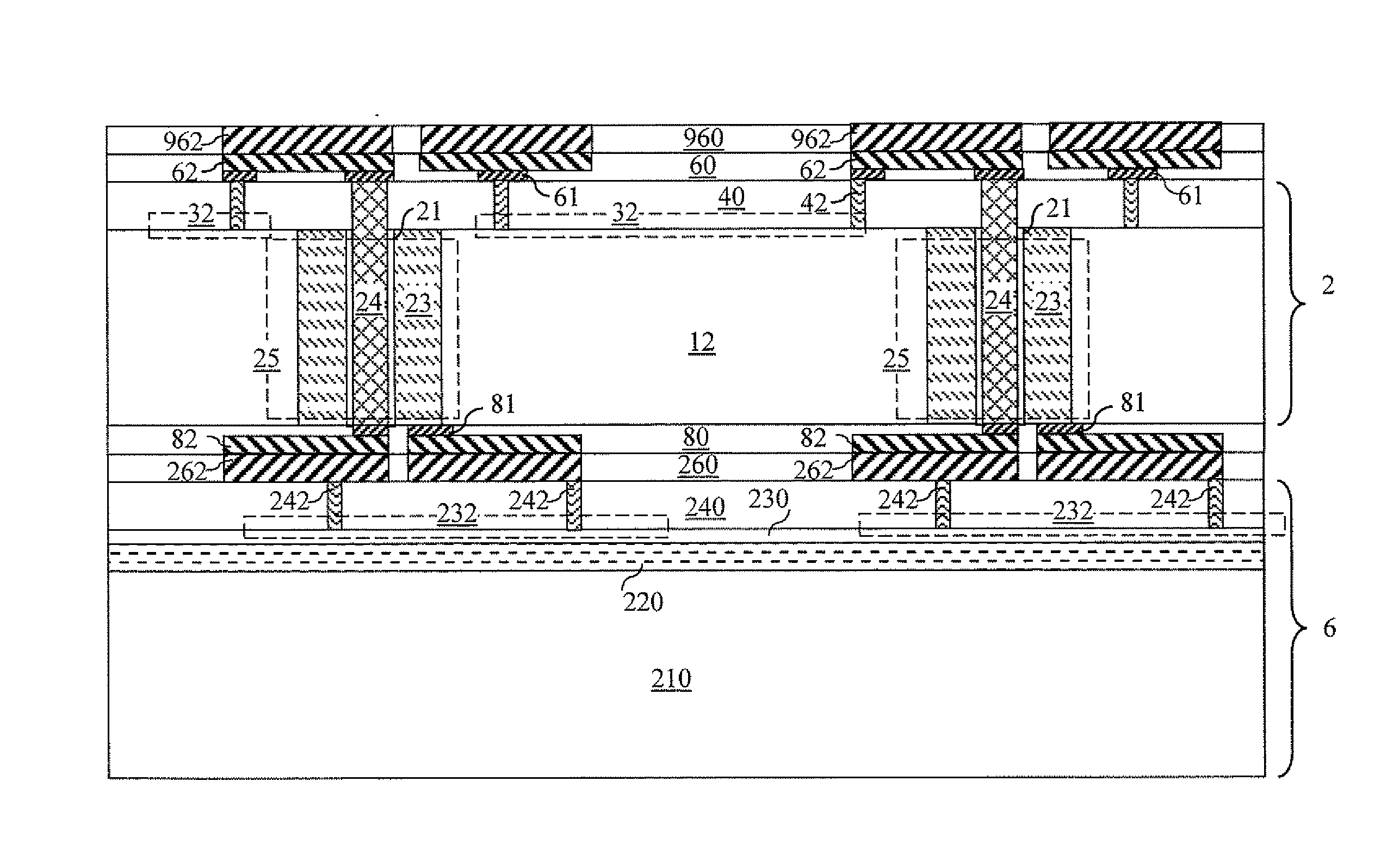
[0059]Referring to FIG. 10, a second exemplary semiconductor structure according to the present invention is derived from the first exemplary structure of FIG. 5 or any variation of the first exemplary structure at a processing step corresponding to the step of FIG. 5 by bonding a temporary substrate 9 to the first substrate 2. The temporary substrate 9 can be bonded to the first substrate 2 by methods known in the art. The first substrate 2 and the temporary substrate 9 collectively constitute a bonded substrate. The front side of the first substrate 2 is bonded to the temporary substrate 9. For example, terminal front side metal pads 962 that are embedded in a terminal front side dielectric layer 960 are formed on the front side of the temporary substrate 9. Subsequently, the terminal front side metal pads 962 in the temporary substrate 9 are bonded to the first front side metal pads 62 in the first substrate 2.

[0060]The temporary substrate 9 includes a temporary handle substrate ...

fourth embodiment

[0080]Referring to FIG. 24, a fourth exemplary semiconductor structure according to the present invention is derived from the third exemplary structure of FIG. 18 by bonding a temporary substrate 9 to the first substrate 2. The temporary substrate 9 can be bonded to the first substrate 2 by methods known in the art. The first substrate 2 and the temporary substrate 9 collectively constitute a bonded substrate. The front side of the first substrate 2 is bonded to the temporary substrate 9. For example, terminal front side metal pads 962 that are embedded in a terminal front side dielectric layer 960 are formed on the front side of the temporary substrate 9. Subsequently, the terminal front side metal pads 962 in the temporary substrate 9 are bonded to the first front side metal pads 62 in the first substrate 2.

[0081]The temporary substrate 9 includes a temporary handle substrate 910, which can include a semiconductor material, a dielectric material, a conductive material, or a combin...


PUM


Abstract

A shielded through-substrate via (TSV) structure includes a first through-substrate via configured to transmit a signal at least from a top surface of a semiconductor device layer in a substrate to a bottommost surface of the substrate. The shielded TSV structure includes at least one second TSV located on the outside of the first TSV and configured to laterally shield the first TSV from external electrical signals. The at least one second TSV can be a unitary cylindrical structure including the first TSV therein, or a plurality of discrete structures configured to laterally shield the first TSV with gaps thereamongst. The at least one second TSV can include a conductive material that is different from the material of the substrate, or the at least one TSV can include a doped semiconductor material that is derived from the semiconductor material within the substrate.

Description

BACKGROUND[0001]The present invention relates to semiconductor structures including a shielded through-substrate via structure and methods of manufacturing the same.[0002]Chip stacking refers to a method of assembling two or more semiconductor chips so that the semiconductor chips that are placed in physical proximity to one another are also electrically connected among one another. Chip stacking is typically performed vertically, i.e., one chip is placed above or below another chip. When two chips are brought together vertically, a set of conductive contact structures on the top surface of an underlying chip is aligned to another set of conductive contact structures on the bottom surface of an overlying chip. The conductive structures may be formed on the side of metal interconnect structures, or they may be formed on the side of a substrate on which semiconductor devices are formed.[0003]3D integration may be performed between a pair of substrates, a substrate and a set of chips, ...

Claims


Application Information

Patent Timeline
Patent Type & Authority Applications(United States)
IPC IPC(8): H01L23/538H01L21/768
CPCH01L21/568H01L21/76898H01L2924/1305H01L2924/1461H01L2924/1301H01L2224/16H01L2924/12044H01L23/481H01L23/552H01L25/0657H01L2225/06513H01L2225/06541H01L2924/00
Inventor KOESTER, STEVEN J.LIU, FEI
Owner GLOBALFOUNDRIES INC
Why Eureka
Try Eureka