Solid-state image capturing device and electronic device

a technology of solid-state image and electronic device, which is applied in the scanning details of television systems, picture signal generators, and the like, can solve the problems of insufficient white and black gradation levels, time shift, and problems that cannot be solved, and achieve the effect of expanding the dynamic range and expanding the dynamic rang

Inactive Publication Date: 2011-10-06
SONY SEMICON SOLUTIONS CORP
View PDF23 Cites 85 Cited by
  • Summary
  • Abstract
  • Description
  • Claims
  • Application Information

AI Technical Summary

Benefits of technology

[0023]With the solid-state image capturing device according to the embodiment of the present invention, since the photochromic film is made of a photochromic material whose light transmittance half-value period is shorter than one frame of the solid-state image capturing device, the solid-state image capturing device has an expanded dynamic range and can generate images free of oddities.
[0024]With the electronic de...

Problems solved by technology

Since the amount of signal charges that can be stored is limited, when intensive light is applied to the sensors, they tend to be saturated making white and black gradation levels insufficient.
Problems that cannot be solved by the above disclosed technologies according to the related art include a time shift that occurs when a moving image is captured or when images are captured in succession.
Accor...

Method used


Image

  • Solid-state image capturing device and electronic device
  • Solid-state image capturing device and electronic device
  • Solid-state image capturing device and electronic device

Examples


first embodiment

[Arrangement of Solid-State Image Capturing Device]

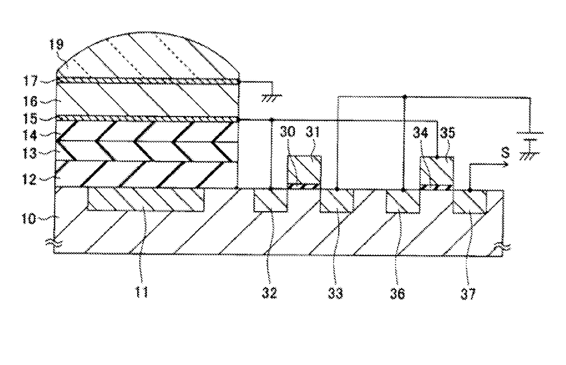
[0077]FIG. 1 is a schematic cross-sectional view of a solid-state image capturing device according to a first embodiment of the present invention.

[0078]As shown in FIG. 1, the solid-state image capturing device includes a matrix of pixels disposed on a semiconductor substrate 10, providing a photosensitive surface. Each of the pixels on the photosensitive surface has a photodiode 11 as a photoelectric converter. In FIG. 1, only one pixel is illustrated.

[0079]The pixel on the photosensitive surface will be described in detail below.

[0080]The photosensitive surface provided on the semiconductor substrate 10 by the photodiode 11 is covered with a first insulating film 12 made of silicon oxide, silicon nitride, or resin, or stacked layers of silicon oxide, silicon nitride, and resin, for example.

[0081]The first insulating film 12 is covered with a second insulating film 13 made of silicon oxide nitride, for example.

[0082]The second insu...

second embodiment

[Arrangement of Solid-State Image Capturing Device]

[0133]FIG. 6 is a schematic cross-sectional view of a solid-state image capturing device according to a second embodiment of the present invention.

[0134]The solid-state image capturing device according to the second embodiment is substantially similar to the solid-state image capturing device according to the first embodiment except that it has a matrix of red, green, and blue pixels.

[0135]In each set of red, green, and blue pixels, a photodiode 11R serving as a photoelectric converter of the red pixel, a photodiode 11G serving as a photoelectric converter of the green pixel, and a photodiode 11B serving as a photoelectric converter of the blue pixel are disposed in the semiconductor substrate 11.

[0136]The solid-state image capturing device according to the second embodiment also includes a color filter 18R, a color filter 18G, and a color filter 18B disposed on the upper electrode 17 in alignment with the photodiode 11R, the photod...

third embodiment

[Arrangement of Solid-State Image Capturing Device]

[0146]FIG. 7 is a schematic cross-sectional view of a solid-state image capturing device according to a third embodiment of the present invention.

[0147]The solid-state image capturing device according to the third embodiment is substantially similar to the solid-state image capturing device according to the second embodiment except that it has different photochromic films made of different materials corresponding respectively to red, green, and blue pixels in each set.

[0148]The red pixel is combined with a photochromic film 16R having light absorbing characteristics corresponding to the wavelength range of the red pixel.

[0149]The green pixel is combined with a photochromic film 16G having light absorbing characteristics corresponding to the wavelength range of the green pixel.

[0150]The blue pixel is combined with a photochromic film 16B having light absorbing characteristics corresponding to the wavelength range of the blue pixel.

[0...


PUM


Abstract

A solid-state image capturing device includes: a semiconductor substrate having a photosensitive surface including a matrix of pixels as respective photoelectric converters; and a photochromic film disposed in a light path through which light is applied to each of the photoelectric converters, the photochromic film being made of a photochromic material having a light transmittance variable depending on the intensity of applied light in a predetermined wavelength range; wherein the light transmittance has a half-value period shorter than one frame during which pixel signals generated by the pixels are read from all the pixels.

Description

BACKGROUND OF THE INVENTION[0001]1. Field of the Invention[0002]The present invention relates to a solid-state image capturing device, a method of manufacturing such a solid-state image capturing device, a method of designing such a solid-state image capturing device, and an electronic device, and more particularly to a solid-state image capturing device having color filters of R (red), G (green), and B (blue), a method of manufacturing such a solid-state image capturing device, a method of designing such a solid-state image capturing device, and an electronic device.[0003]2. Description of the Related Art[0004]Electronic devices such as electronic digital video devices and electronic digital still devices have a solid-state image capturing device which may include a CCD (Charge Coupled Device) image sensor, a CMOS (Complementary Metal-Oxide-Silicon Transistor) image sensor, or the like.[0005]The solid-state image capturing device includes a matrix of pixels arrayed in horizontal an...

Claims


Application Information

Patent Timeline
IPC IPC(8): H04N5/228H04N5/335
CPCH01L27/14621H01L27/14685H01L27/14625
Inventor IZUHA, KYOKOHARADA, KOUICHI
Owner SONY SEMICON SOLUTIONS CORP
Why Eureka
Try Eureka