Semiconductor device and data processing system

a semiconductor device and data processing technology, applied in the field of semiconductor devices and data processing systems, can solve the problems of inability to achieve the desired characteristics of the sense amplifier, the sensing margin thereof decreases, etc., and achieves excellent sensing margin, prevent the effect of reducing the sensing margin, and increase the capacity of the semiconductor devi

Inactive Publication Date: 2011-10-13
PS4 LUXCO SARL
View PDF7 Cites 3 Cited by
  • Summary
  • Abstract
  • Description
  • Claims
  • Application Information

AI Technical Summary

Benefits of technology

[0010]As described above, according to the present invention, the potential of the driving signal for the gated diode is appropriately controlled corresponding to the fluctuation of the threshold voltage of the gated diode (first FET) connected to the first node as an input node of the amplifier, and thereby it is possible to prevent a decrease in sensing margin due to the fluctuation of the threshold voltage. Particularly, even when random variation of the threshold voltage increases due to a decrease in size and an increase in capacity of a semiconductor device such as a DRAM, the fluctuation caused by manufacturing process or temperature dependence can be reliably compensated and excellent sensing margin can be obtained.

Problems solved by technology

If the threshold voltage of a field-effect transistor functioning as the above gated diode fluctuates due to manufacturing process or temperature dependence, there arises a problem that sensing margin thereof decreases.
Therefore, there arises a problem that it is not possible to achieve desired characteristics of the sense amplifier or the data amplifier to which the above conventional configuration is applied.

Method used


Image

  • Semiconductor device and data processing system
  • Semiconductor device and data processing system
  • Semiconductor device and data processing system

Examples


first embodiment

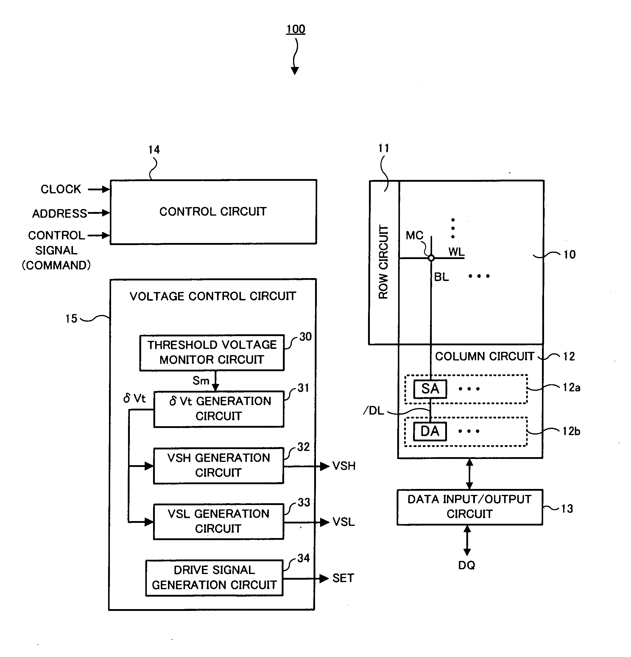
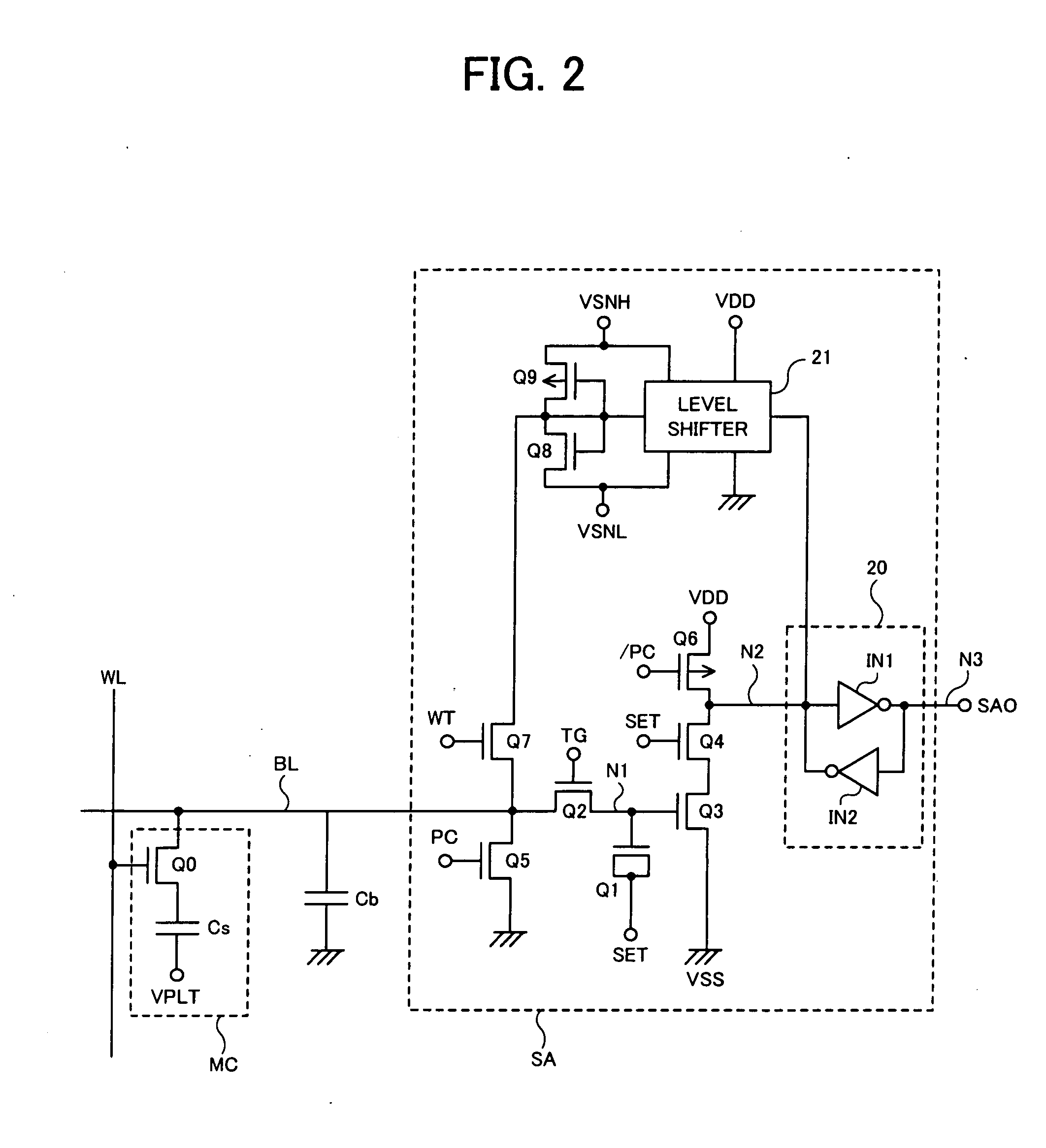
[0035]A DRAM of a first embodiment to which the present invention is applied will be described. FIG. 1 is a block diagram showing a schematic configuration of the DARM of the first embodiment, which shows a semiconductor device 100 including a memory cell array region 10, row circuits 11 and column circuits 12 on the periphery of the memory cell array region 10, a data input / output circuit 13, a control circuit 14 and a voltage control circuit 15. In the memory cell array region 10, a plurality of memory cells MC are formed at intersections of a plurality of word lines WL and a plurality of bit lines BL. The row circuits 11 include circuits associated with the word lines WL, and, for example, a plurality of word drivers (not shown) driving the plurality of word lines WL and the like are provide therein. The column circuits 12 includes circuits associated with the bit lines BL, and, for example, a sense amplifier array 12a including a plurality of sense amplifier SA connected to the ...

second embodiment

[0063]A DRAM of a second embodiment to which the present invention is applied will be described. Although voltage control conditions in the second embodiment are different from those in the first embodiment, the entire configuration of the DRAM of FIG. 1 and the circuit configuration of the sense amplifier SA and its peripheral portion of FIG. 2 are the same as in the first embodiment and thus description thereof will be omitted. In the following, an operation in which data stored in the memory cell MC is read out in the sense amplifier SA of the second embodiment will be described with reference to FIGS. 10 and 11.

[0064]Next, FIG. 10 shows an operation waveform diagram in a case where the operating temperature T is maximum (MAX: 125 degrees Celsius, for example), the manufacturing process is fast speed (FAST), and the variation range Ra of the threshold voltage Vt1 is shifted downward from the typical, similarly as in FIG. 4. Although the offset control in the first embodiment is p...

third embodiment

[0069]A DRAM of a third embodiment to which the present invention is applied will be described. Although the first and second embodiments have described that the invention is applied to the sense amplifier SA of the DRAM, the third embodiment will describe that the invention is applied to a data amplifier DA of the DRAM. The DRAM of the third embodiment has the same entire configuration as that in FIG. 1 of the first embodiment and thus description thereof will be omitted. In the third embodiment, portions different from the first embodiment will be mainly described.

[0070]FIG. 13 shows a circuit configuration of the data amplifier DA and its peripheral portion in the third embodiment. In FIG. 13, a read circuit portion SAR (the first circuit of the invention) of the sense amplifier SA, and a single-ended data amplifier DA connected to the read circuit portion SAR via a data line / DL (the first signal line of the invention). The read circuit portion SAR of the sense amplifier SA is c...


PUM


Abstract

A semiconductor device comprises a first circuit outputting a signal to a first signal line, a first FET applied with a driving signal and having a gate electrode connected to a first node, a second FET controlling an electrical connection between the first signal line and the first node, a third FET amplifying a signal of the first node, a second circuit precharging the first signal line, and a voltage control circuit. A gate capacitance of the first FET is controlled in response to a voltage difference between the first node and the driving signal. The voltage control circuit shifts a potential of the driving signal when the second FET is non-conductive after the signal of the first-circuit is transmitted to the first node, and performs an offset control for the driving signal so as to compensate a variation of a threshold voltage of the first FET.

Description

BACKGROUND OF THE INVENTION[0001]1. Field of the Invention[0002]The present invention relates to a semiconductor device provided with an amplifier that senses and amplifies a signal voltage transmitted through a signal line. For example, the present invention relates to a semiconductor device provided with a single-ended sense amplifier that senses and amplifies data read out from a memory cell through a bit line or provided with a single-ended data amplifier that senses and amplifies the data of the sense amplifier read out thorough a data line.[0003]2. Description of Related Art[0004]In recent years, a decrease in size and an increase in capacity have been achieved in a semiconductor device such as a DRAM, and therefore it is desirable to employ a single-ended circuit configuration with a small circuit scale and a dense arrangement as an amplifier such as a sense amplifier or a data amplifier. For example, an amplifier using a so-called gated amplifier is proposed as a single-ende...

Claims


Application Information

Patent Timeline
Patent Type & Authority Applications(United States)
IPC IPC(8): G05F3/08
CPCG11C5/147G11C11/4091G11C7/04
Inventor KAJIGAYA, KAZUHIKOYOSHIDA, SOICHIROYAMADA, YASUTOSHI
Owner PS4 LUXCO SARL
Why Eureka
Try Eureka