Semiconductor device and data processing system

a semiconductor device and data processing technology, applied in the field of semiconductor devices, can solve the problems of inability to adapt, inability to effectively prevent a performance deterioration of the sense amplifier, and difficulty in obtaining a sufficient capacitance of the capacitor included in each memory cell, so as to achieve excellent sensing margin, effectively prevent a decrease in sensing margin, and increase the capacity of the semiconductor device

Inactive Publication Date: 2013-04-16
LONGITUDE SEMICON S A R L
View PDF17 Cites 7 Cited by
  • Summary
  • Abstract
  • Description
  • Claims
  • Application Information

AI Technical Summary

Benefits of technology

[0015]According to the semiconductor device of the invention, for example, the first transistor of the single-ended sense amplifier functions as a charge transfer switch between the bit line and the input node of the sense amplifier, and by controlling the potential of the transfer control signal applied to its gate, it is possible to prevent an operation failure due to a variation distribution of the threshold voltage of the first transistor. In this case, a plurality of reference voltages associated with the variation distribution of the threshold voltage are provided, one reference voltage suitable for a predetermined number of the sense amplifiers is selected among them, and control is performed so that the selected reference voltage is used as the potential of the transfer control signal in an activated state. Thus, sensing margin for the predetermined number of the sense amplifiers can be optimized, and the operating failure due to the variation distribution of the threshold voltage can be prevented.
[0017]As described above, the present invention is applied to a semiconductor device such as DRAM in which a large number of transmission lines and corresponding sense amplifiers are provided. When a single-ended sense amplifier is employed in the semiconductor device, in consideration of the variation distribution of the threshold voltage of the first transistor as the charge transfer switch of the sense amplifier, the reference voltage applied to the gate of the first transistor is controlled within a range of a predetermined voltage width (for example, the potential of the transfer controls signals is controlled in accordance with a reference voltage selected among the plurality of reference voltages). Therefore, the operation failure due to the variation distribution of the threshold voltage of the first transistor is prevented by the controlled reference voltage, thereby obtaining excellent sensing margin. Further, even when the variation distribution of the first transistor of the sense amplifier increases in the chip due to a decrease in size and an increase in capacity of the semiconductor device such as DRAM, it is possible to effectively prevent a decrease in sensing margin.

Problems solved by technology

In recent years, as miniaturization of memory cells has been advanced in semiconductor memory devices such as DRAM, it becomes difficult to obtain a sufficient capacitance of a capacitor included in each memory cell.
However, the above conventional offset compensation technique associated with the random variation of the threshold voltages of transistors is adapted to the differential type sense amplifier (configured to have two input terminals, one of which is a first input terminal receiving signal data of a transmission line, and the other of which is a second input terminal receiving a reference signal for sensing), and cannot be adapted to the single-ended sense amplifier (configured to have one input terminal).
As described above, in case of configuring a semiconductor device by employing the single-ended sense amplifiers, there has not been proposed a method to effectively prevent a performance deterioration of the sense amplifier due to the variation distribution of the threshold voltages of field-effect transistors (for example, MOS transistors).

Method used


Image

  • Semiconductor device and data processing system
  • Semiconductor device and data processing system
  • Semiconductor device and data processing system

Examples


Embodiment Construction

[0035]A typical example of a technical idea solving the problems of the present invention will be shown below. However, It goes without saying that the present invention is not limited to the example of the technical idea and should be construed based on the disclosure of the claims.

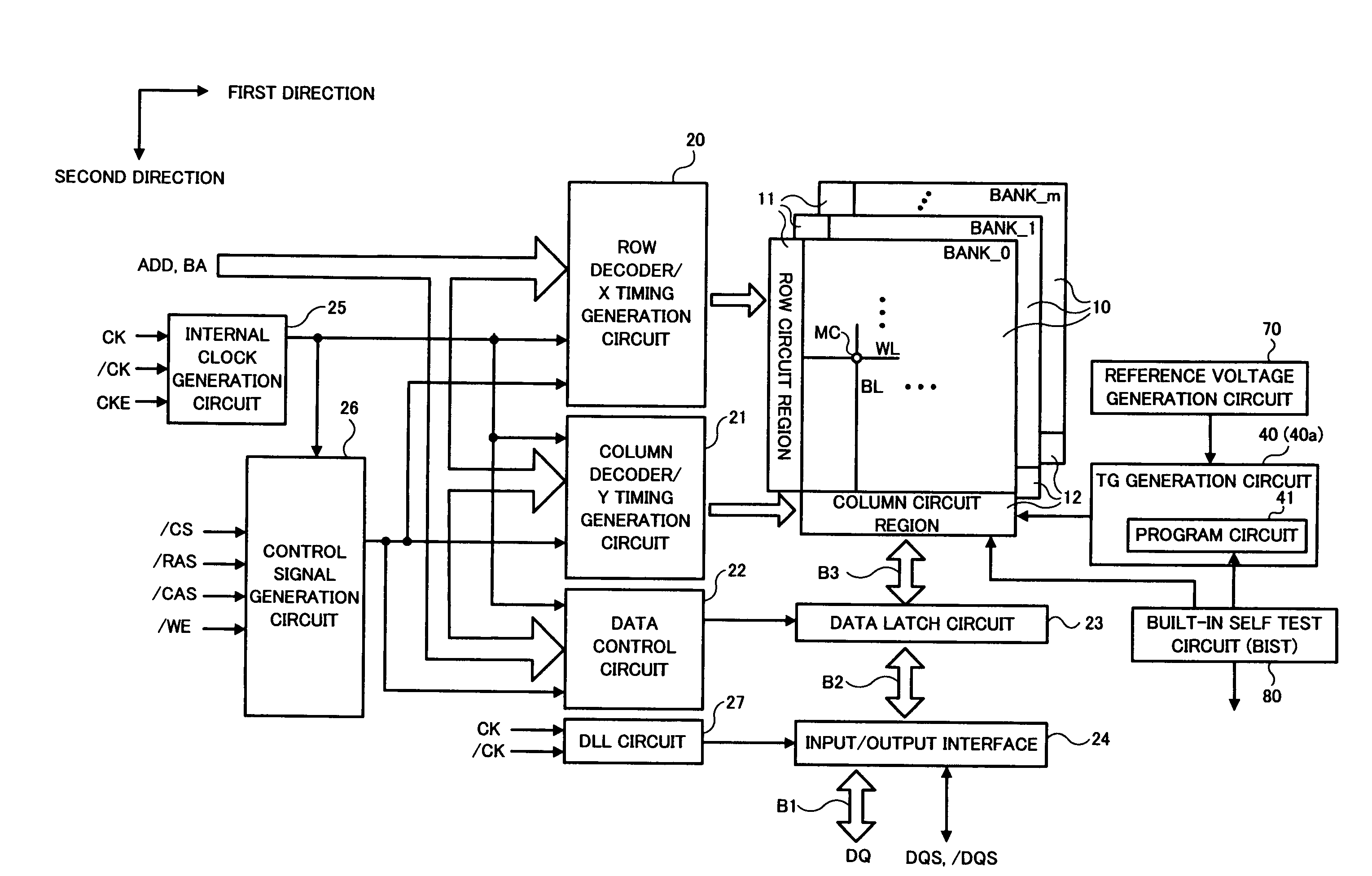
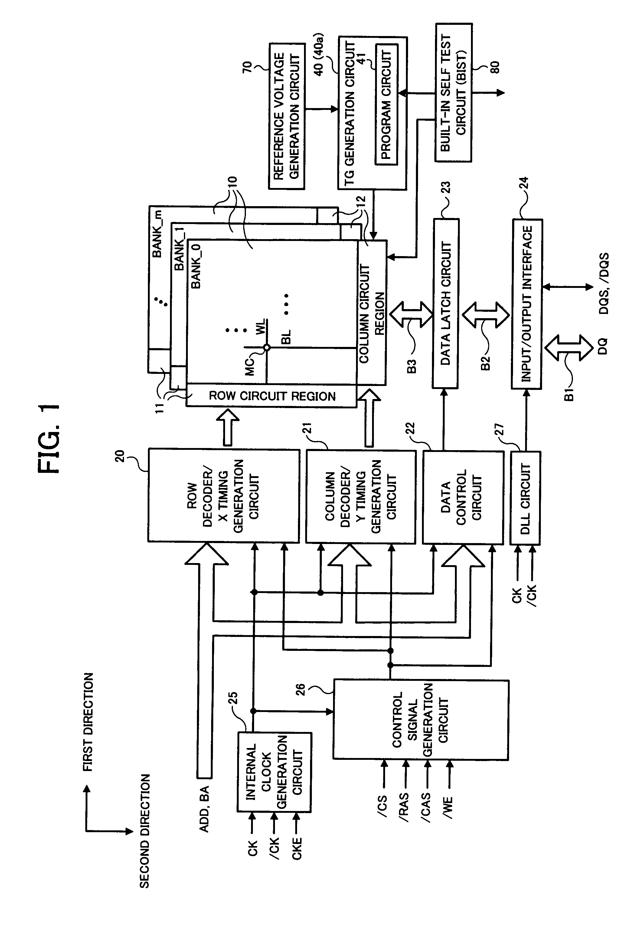
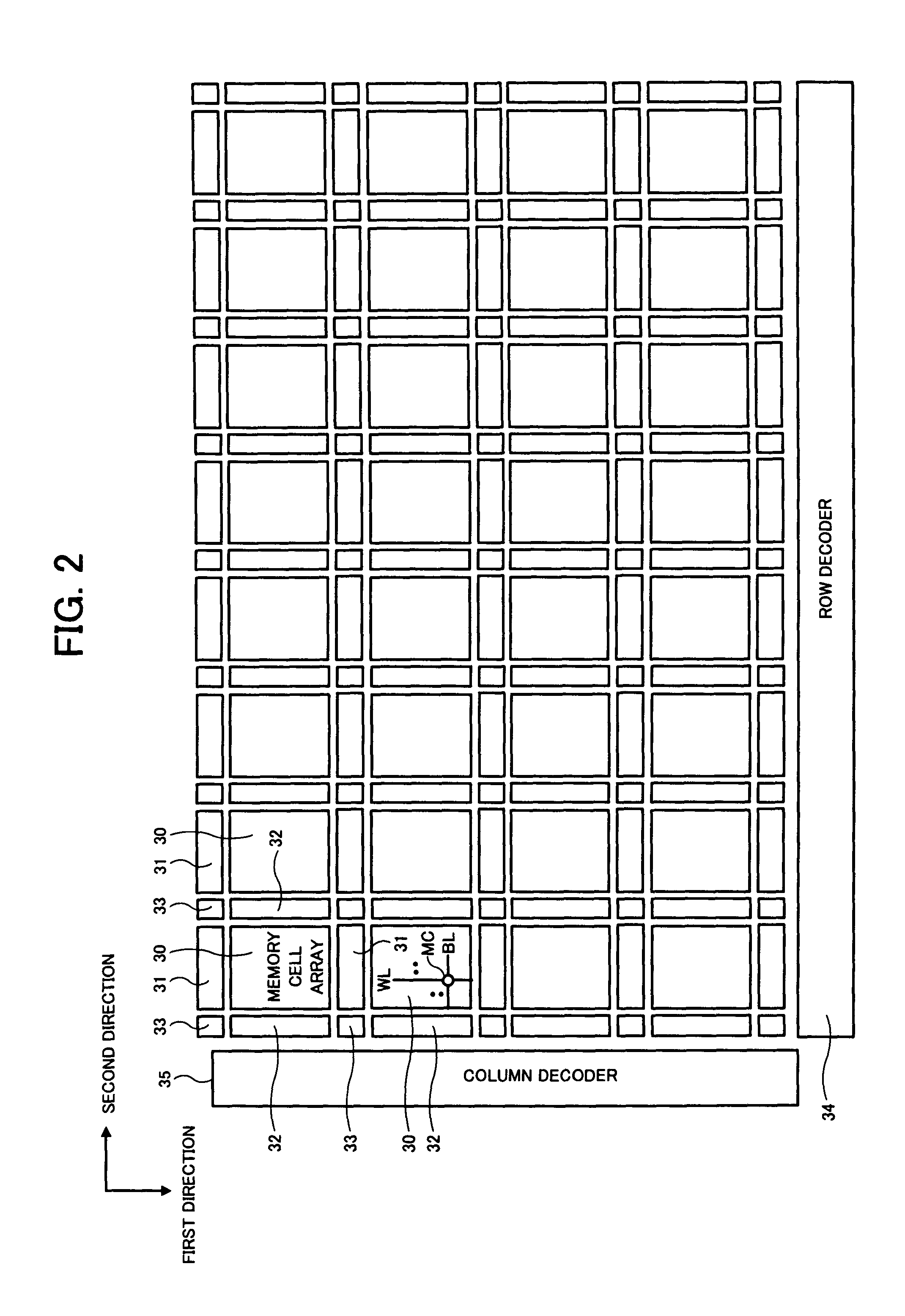
[0036]An example of the technical idea of the invention is applied to a predetermined number of single-ended sense amplifiers (for example, one sense amplifier row) included in a semiconductor device, in which the potential of a transfer control signal in an activated state applied to the gate of a first transistor for charge transfer of a sensed signal between a bit line as a transmission line and an input node of the sense amplifier is controlled within a range of a predetermined voltage width (controlled to be a reference voltage selected among a plurality of reference voltages). Since the plurality of reference voltages are set corresponding to a variation distribution of the threshold voltage of the...


PUM


Abstract

A semiconductor device comprises a bit line transmitting a signal to be sensed, a single-ended sense amplifier sensing and amplifying the signal transmitted from the bit line to the input node, and a reference voltage supplying circuit outputting a reference voltage. The sense amplifier includes a first transistor for charge transfer between the bit line and an input node, and the voltage value of the reference voltage is controlled in association with a threshold voltage of the first transistor. The reference voltage is set to a first logical value of the transfer control signal which controlled to be first and second logical values.

Description

BACKGROUND OF THE INVENTION[0001]1. Field of the Invention[0002]The present invention relates to a semiconductor device provided with a single-ended sense amplifier that senses data on a transmitted line, and particularly relates to a semiconductor device in which data stored in a memory cell is read out to a bit line and amplified by the single-ended sense amplifier.[0003]2. Description of Related Art[0004]In recent years, as miniaturization of memory cells has been advanced in semiconductor memory devices such as DRAM, it becomes difficult to obtain a sufficient capacitance of a capacitor included in each memory cell. Therefore, a sense amplifier capable of reliably amplifying a minute signal voltage readout from the memory cell is desired. For example, a charge transfer type sense amplifier is known as an example of the sense amplifier suitable for amplifying the minute signal voltage (for example, refer to the following Patent References 1 to 4). In general, a differential type ...

Claims


Application Information

Patent Timeline
Patent Type & Authority Patents(United States)
IPC IPC(8): G11C5/14
CPCG11C5/14G11C7/00G11C11/4091G11C7/08G11C7/065G11C7/04G11C16/28G11C7/14G11C29/028G11C5/147
Inventor KAJIGAYA, KAZUHIKO
Owner LONGITUDE SEMICON S A R L
Why Eureka
Try Eureka