Nanostructured LED

Active Publication Date: 2011-10-20
NANOSYS INC
View PDF12 Cites 151 Cited by
  • Summary
  • Abstract
  • Description
  • Claims
  • Application Information

AI Technical Summary

Benefits of technology

[0011]One further object of the invention is to provide a nanowire LED comprising one or more contact groups of nanowires that can be exclusively and individually addressed.
[0012]Embodiments of the invention are defined in the dependent claims. Other objects, advantages and novel features of the invention will become apparent from the following detailed description of examples of embodiments of the invention when considered in conjunction with the accompanying drawings and claims.

Problems solved by technology

The prior art has drawbacks with regard to being able to provide a nanostructured LED having high efficiency and being suitable for large scale production.

Method used


Image

  • Nanostructured LED
  • Nanostructured LED
  • Nanostructured LED

Examples


Embodiment Construction

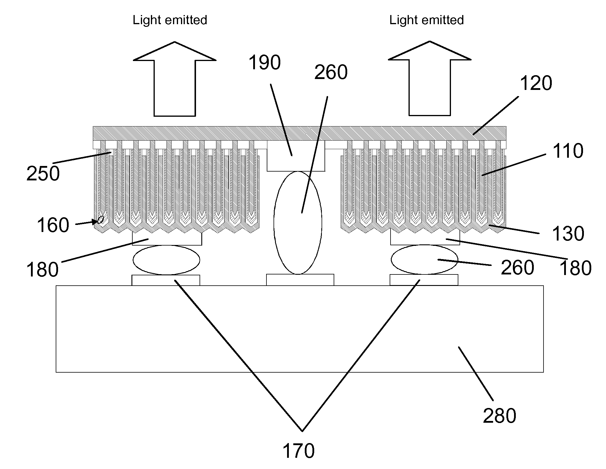
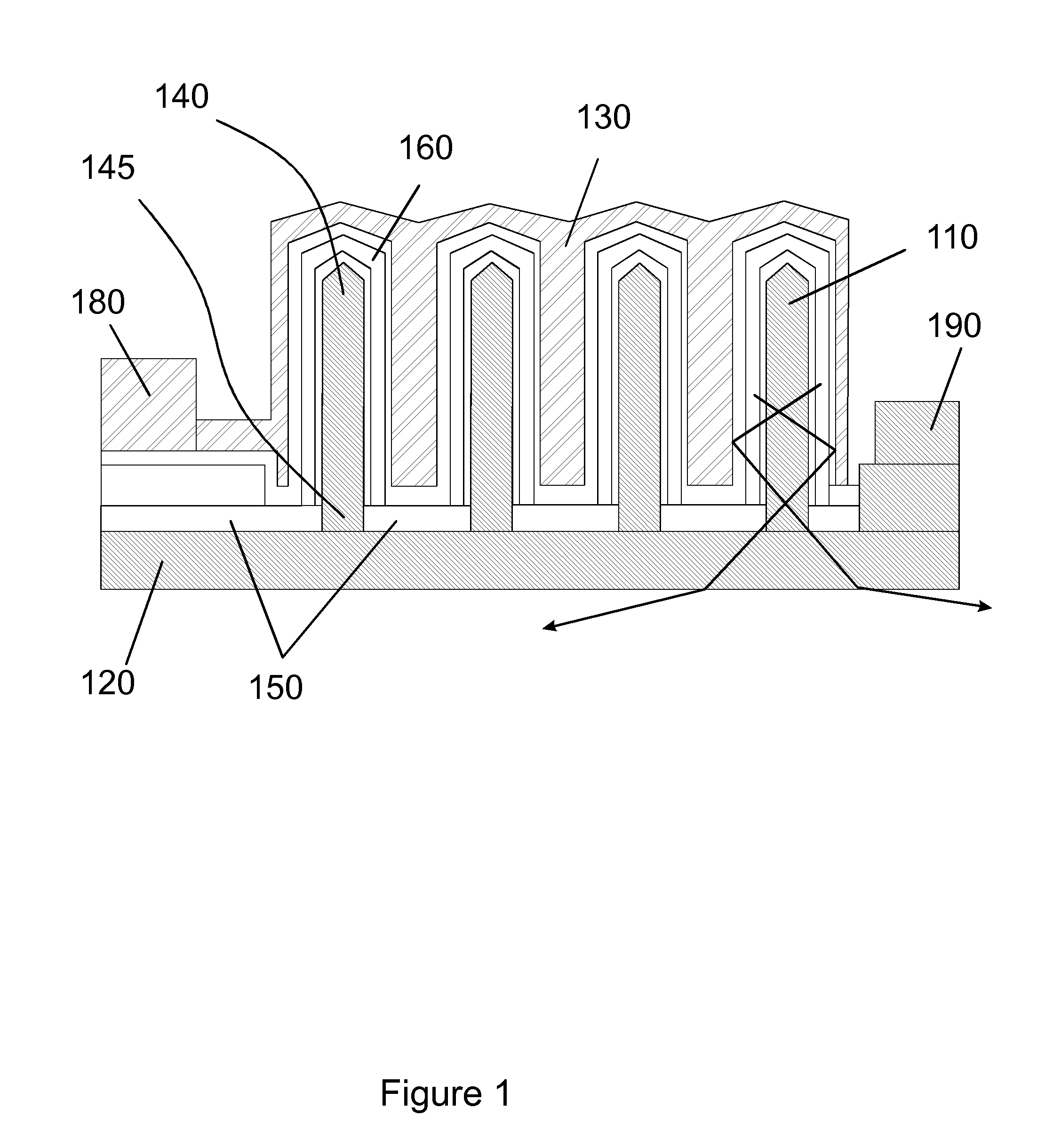
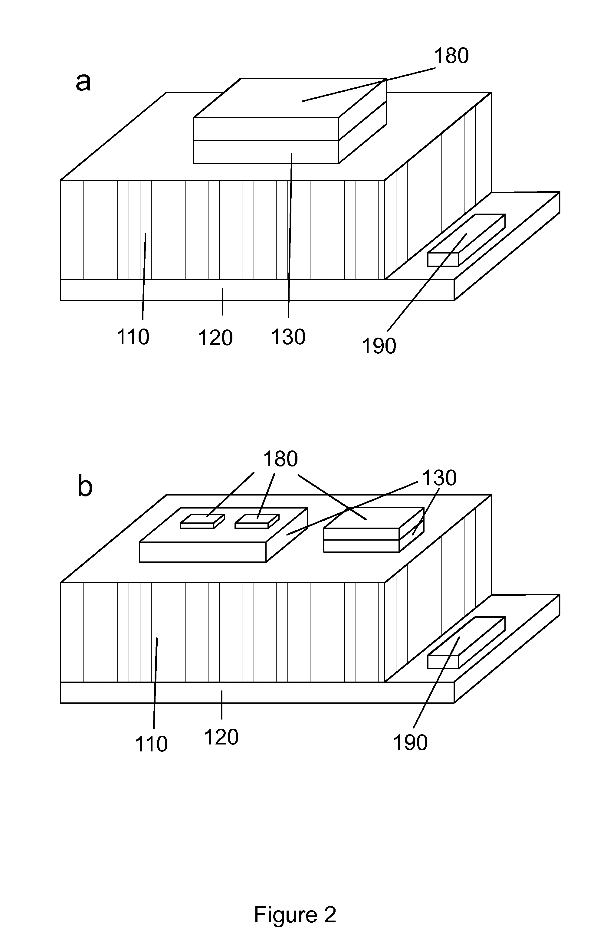
[0023]The embodiments to be described in the following are all based on nanostructured LED / LED's, and a prior art version of such can be found in WO2008048704.

[0024]In the following discussion the term nanostructure or nanoelement is intended to mean a structure having at least two dimensions not greater than about 1 μm.

[0025]In one embodiment, FIG. 1, of a nanostructured LED according to the invention, the nanowires 110 protrude from a substrate or a buffer layer 120 deposited on a substrate (the substrate not shown in the figure), where the substrate or buffer layer 120 can be Si, Ge, Al2O3, SiC, Quartz, glass, GaN or any other material suitable for nanowire growth and further processing. The buffer layer 120 can be made of a material different than the substrate material. The buffer layer 120 is usually chosen so as to match the desired nanowire material, and thus form a growth base for the nanowires later in the process. That means that the buffer layer 120 is chosen so that the...


PUM

PropertyMeasurementUnit
transparentaaaaaaaaaa
serial resistanceaaaaaaaaaa
electrical current transportaaaaaaaaaa

Abstract

The device according to the invention comprises a nanostructured LED with a first group of nanowires protruding from a first area of a substrate and a contacting means in a second area of the substrate. Each nanowire of the first group of nanowires comprises a p-i-n junction and a top portion of each nanowire or at least one selection of nanowires is covered with a light-reflecting contact layer. The contacting means of the second area is in electrical contact with the bottom of the nanowires, the light-reflecting contact layer being in electrical contact with the contacting means of the second area via the p-i-n junction. Thus when a voltage is applied between the contacting means of the second area and the light-reflecting contact layer, light is generated within the nanowire. On top of the light-reflecting contact layer, a first group of contact pads for flip-chip bonding can be provided, distributed and separated to equalize the voltage across the layer to reduce the average serial resistance.

Description

TECHNICAL FIELD OF THE INVENTION[0001]The present invention relates to LEDs. In particular the invention relates to nanostructured LEDs.BACKGROUND OF THE INVENTION[0002]Nanowire based LEDs (Light Emitting Diodes) are comprised of semiconductor nanowires or arrays of semiconductor nanowires grown on a substrate, like for example silicon or GaN. Typically on such substrate a planar buffer layer is grown first and subsequently an array of nanowires is grown on the surface of the buffer layer. The buffer layer is used as the base layer for growing the nanowires. Additionally, it can serve for electrical current transport. The buffer layer is usually transparent for the light emitted by the LED.[0003]Each nanowire protrudes from the buffer layer and contains multiple regions of materials forming p-i-n junctions around the nanowire core or along the nanowire axis. When charge carriers are injected into the respective p- and n-regions, they recombine in the i-region, and this recombination...

Claims


Application Information

Patent Timeline
Patent Type & Authority Applications(United States)
IPC IPC(8): H01L33/60B82Y20/00
CPCB82Y20/00H01L33/24H01L33/08H01L33/20H01L33/32H01L33/38H01L33/40H01L33/60H01L33/62Y10S977/762Y10S977/95F21S48/115F21Y2105/001F21S48/1747H01L2924/0002H01L27/153H01L33/18H01L2924/00H01L27/156F21Y2105/10F21Y2115/10F21S41/663F21S41/153B82B1/00H01L33/04H01L33/387
Inventor KONSEK, STEVENOHLSSON, JONASMARTYNOV, YOURIIHANBERG, PETER
Owner NANOSYS INC
Why Eureka
Try Eureka