Current measurement method, inspection method of semiconductor device, semiconductor device, and test element group

a technology of inspection method and semiconductor device, which is applied in the direction of measurement device, electrical measurement, instruments, etc., can solve the problems of delay in developing electrical elements, development of devices or circuits based on new characteristic values, and inability to know their precise value, so as to achieve the effect of easy control of the potential of the node and increase the yield of the semiconductor devi

Active Publication Date: 2011-10-20
SEMICON ENERGY LAB CO LTD
View PDF2 Cites 17 Cited by
  • Summary
  • Abstract
  • Description
  • Claims
  • Application Information

AI Technical Summary

Benefits of technology

[0018]In the above, a capacitor can be connected to the node, thereby offering the advantage that the potential of the node is easily controlled.
[0019]It is possible to examine whether or not a transistor for evaluation has predetermined characteristics using the above current measurement method. Consequently, defects in a manufactured semiconductor device can be detected. Further, it is also possible to design a semiconductor device using a characteristic value measured by this inspection method. Consequently, yield of a semiconductor device can be increased.
[0030]Further, by examining whether or not an electrical element has predetermined characteristics using the above current measurement method, defects in a manufactured semiconductor device can be accurately detected.

Problems solved by technology

For this reason, if the off-state current is lower than the lowest detection limit, it has been difficult to know its precise value.
Such a situation might cause a delay in developing electrical elements typified by thin film transistors.
If the transistor characteristics cannot be precisely measured, the development of devices or circuits based on new characteristic values and the development of application products do not progress.

Method used


Image

  • Current measurement method, inspection method of semiconductor device, semiconductor device, and test element group
  • Current measurement method, inspection method of semiconductor device, semiconductor device, and test element group
  • Current measurement method, inspection method of semiconductor device, semiconductor device, and test element group

Examples


embodiment 1

[0057]In this embodiment, an example of a current measurement method according to one embodiment of the disclosed invention and a measurement system used for the current measurement method will be described with reference to FIG. 1.

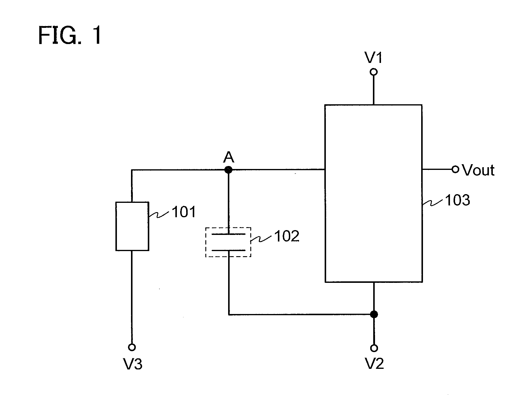
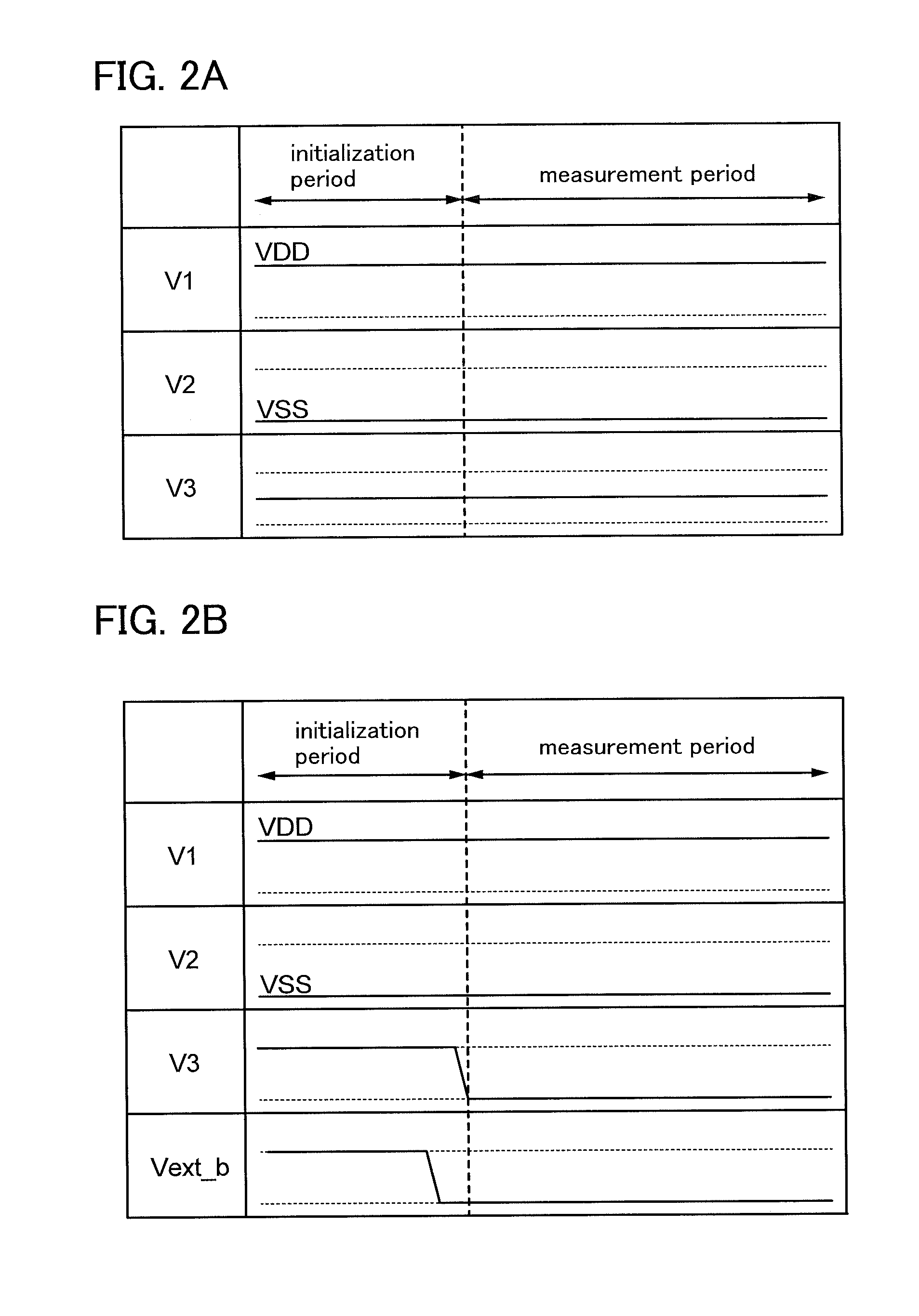
[0058]First, one example of a measurement system used for the current measurement method according to one embodiment of the disclosed invention will be described with reference to FIG. 1. The configuration of a measurement system below can be used as the configuration of a TEG Note that the measurement system described below is only an example, and the disclosed invention should not be construed as being limited thereto.

[0059]A measurement system illustrated in FIG. 1 includes an electrical element 101, a capacitor 102, and an output circuit 103. The electrical element 101 has a first terminal and a second terminal. The capacitor 102 has a first terminal and a second terminal. The output circuit 103 has an input terminal, an output terminal, a first termi...

embodiment 2

[0082]In this embodiment, other examples of the measurement system described in the above embodiment will be described with reference to FIGS. 4A to 4C, FIG. 5, FIG. 6, and FIGS. 7A and 7B. The configuration of a measurement system below can be used as the configuration of a TEG. Note that the measurement system below is only an example, and the disclosed invention should not be construed as being limited thereto.

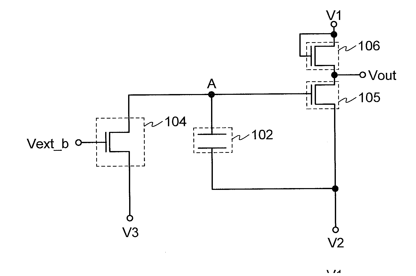
[0083]A measurement system illustrated in FIG. 4A includes a capacitor 102, a transistor 104, a transistor 105, and a transistor 106. Here, the transistor 104 corresponds to the electrical element 101 in FIG. 1. Further, the transistor 105 and the transistor 106 constitute a circuit corresponding to the output circuit 103 in FIG. 1.

[0084]In FIG. 4A, a source terminal (or a drain terminal) of the transistor 104 corresponds to the first terminal of the electrical element 101 in FIG. 1. Further, the drain terminal (or the source terminal) of the transistor 104 corresponds to t...

embodiment 3

[0107]In this embodiment, other examples of the measurement system described in the above embodiments will be described with reference to FIG. 8, FIG. 9, and FIG. 10. The configuration of a measurement system below can be used as the configuration of a TEG.

[0108]A measurement system illustrated in FIG. 8 has a structure partly different from that illustrated in FIG. 1. Portions different from those in FIG. 1 will be described. A structure illustrated in FIG. 8 includes, in addition to the components illustrated in FIG. 1, an electrical element 109. The electrical element 109 has a first terminal and a second terminal.

[0109]In FIG. 8, the second terminal of the electrical element 101 is connected to the first terminal of the electrical element 109, the first terminal of the capacitor 102, and the input terminal of the output circuit 103. The second terminal of the electrical element 109 is connected to a power source or a signal source. The first terminal of the electrical element 10...


PUM


Abstract

One object is to provide a method for measuring current by which minute current can be measured. A value of current flowing through an electrical element is not directly measured but is calculated from change in a potential observed in a predetermined period. The method for measuring current includes the steps of: applying a predetermined potential to a first terminal of an electrical element having the first terminal and a second terminal; measuring an amount of change in a potential of a node connected to the second terminal; and calculating, from the amount of change in the potential, a value of current flowing between the first terminal and the second terminal of the electrical element. Thus, the value of minute current can be measured.

Description

BACKGROUND OF THE INVENTION[0001]1. Field of the Invention[0002]The disclosed invention relates to a method for measuring a minute current flowing through an electrical element, an inspection method of a semiconductor device employing the current measurement method, a semiconductor device employing the current measurement method, a semiconductor device employing the inspection method, a test element group (also referred to as a TEG), and the like. Here, a semiconductor device may be any device which works by utilizing semiconductor characteristics. For example, a semiconductor device widely includes the following elements: a semiconductor element (including a so-called power device) such as a transistor, a diode, and a thyristor, an integrated circuit such as an image sensor, a memory, and a converter, an integrated circuit including the above elements, and a display device and the like typified by a liquid crystal display device.[0003]2. Description of the Related Art[0004]In recen...

Claims


Application Information

Patent Timeline
Patent Type & Authority Applications(United States)
IPC IPC(8): G01R19/00
CPCG01R31/2601G01R19/0092
Inventor KATO, KIYOSHISEKINE, YUSUKESHIONOIRI, YUTAKAFURUTANI, KAZUMA
Owner SEMICON ENERGY LAB CO LTD
Why Eureka
Try Eureka