Light emitting diode package and manufacturing method thereof
a technology of light-emitting diodes and manufacturing methods, applied in the direction of semiconductor devices, basic electric elements, electrical apparatus, etc., can solve the problems of time-consuming, complicated method for manufacturing metal reflectors, and restricting light-emitting efficiency
- Summary
- Abstract
- Description
- Claims
- Application Information
AI Technical Summary
Benefits of technology
Problems solved by technology
Method used
Image
Examples
first embodiment
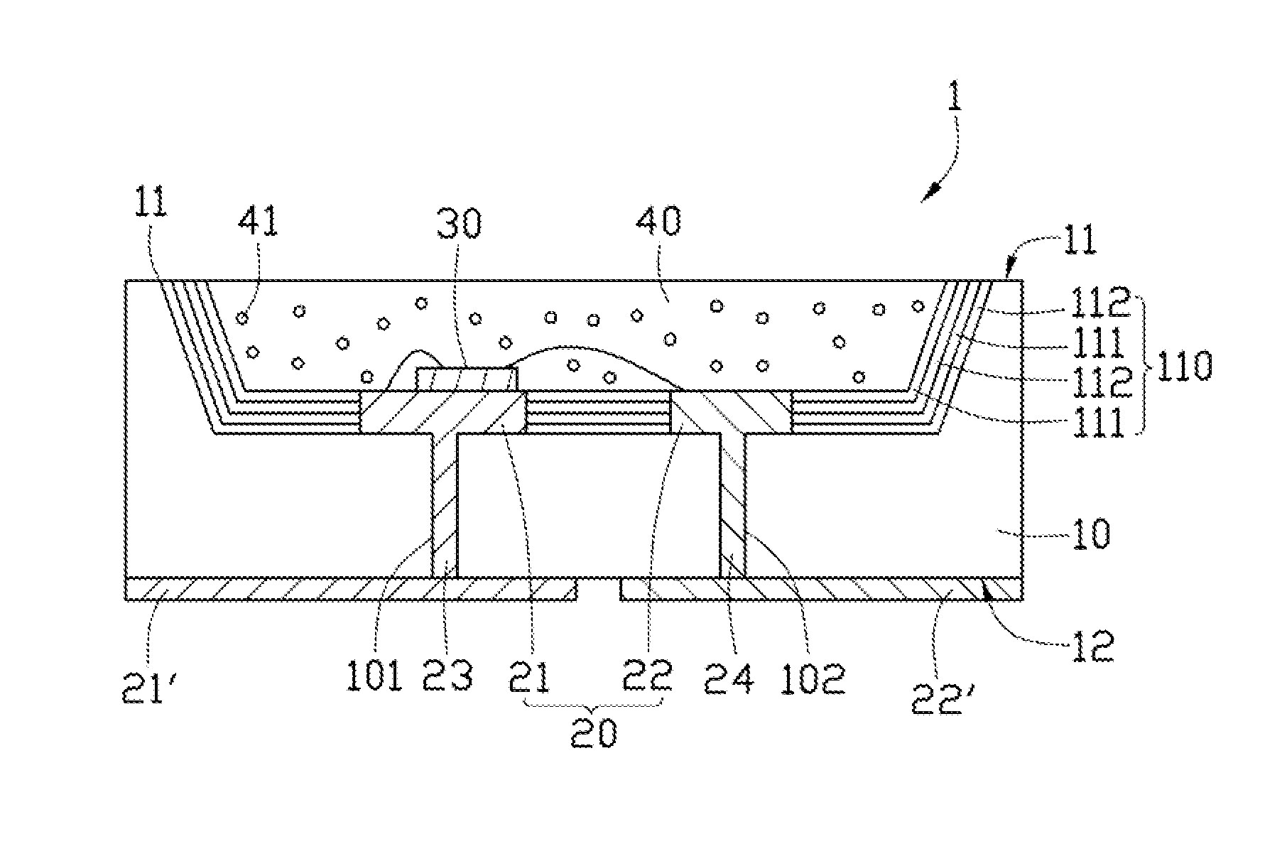
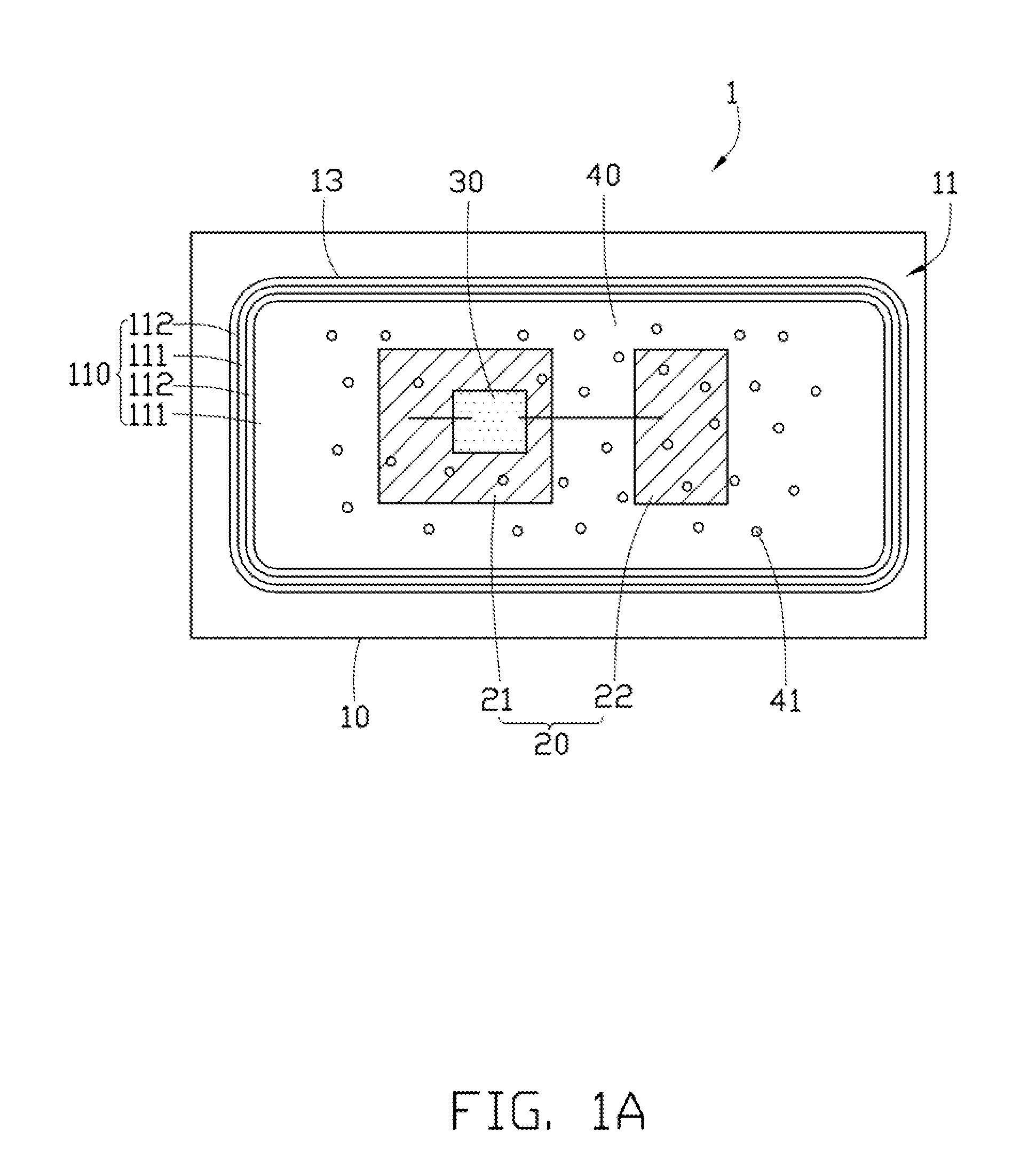
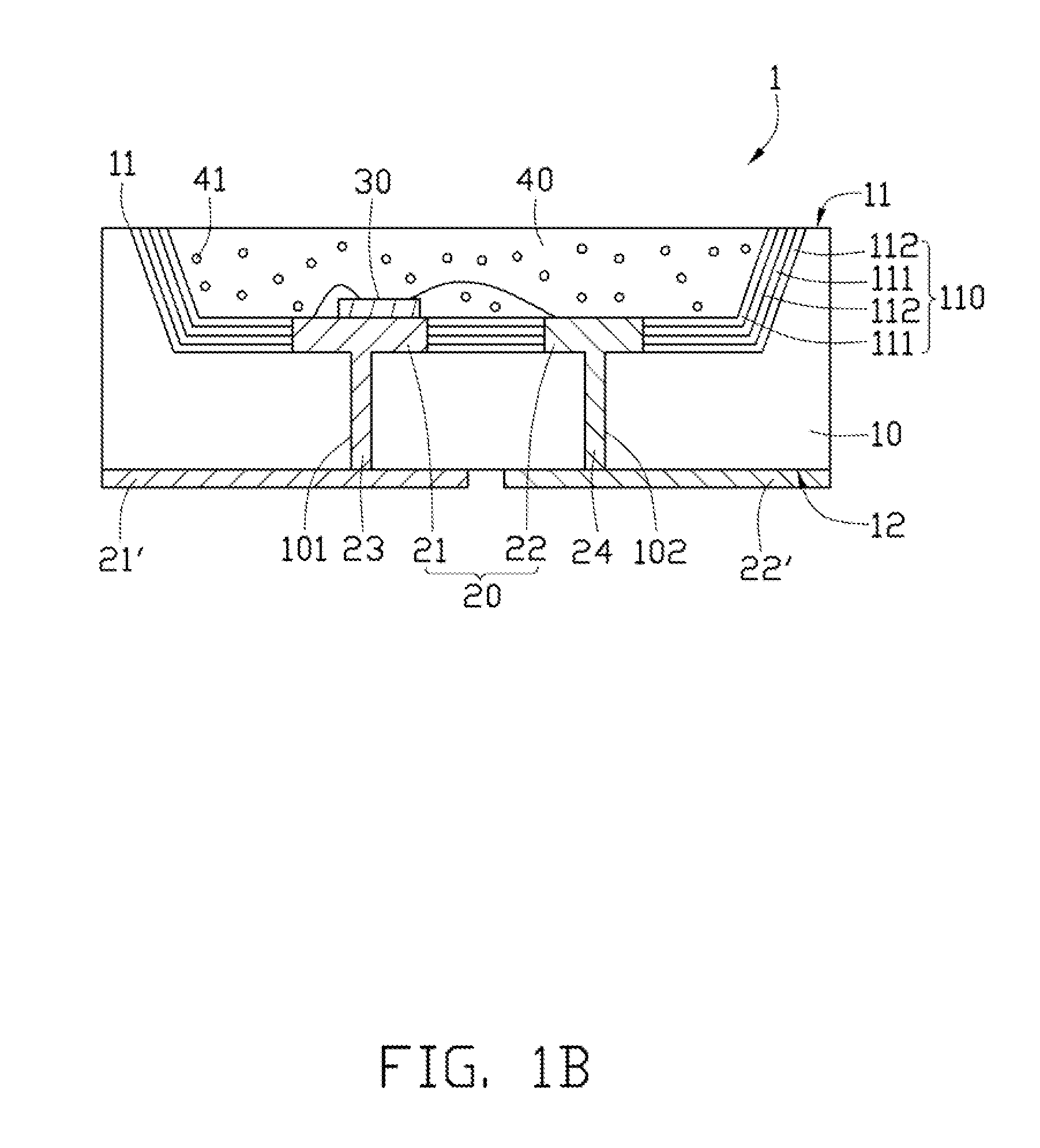
Referring to FIGS. 1A and 1B, the disclosure provides a light emitting diode package 1 comprising a substrate 10, a lead frame 20, a light emitting device 30 and an encapsulation 40, wherein the light emitting device 30 is capable of emitting light of a first wavelength.
The substrate 10 comprises a first surface 11 and a second surface 12 opposite to each other. A depression 13 is allocated upon the first surface 11, in which the light emitting device 30 is disposed. In the disclosure, the substrate 10 is silicon, ceramic, metal or polymer, and the depression 13 is formed by wet-etching, dry-etching, mechanic or laser. The depression 13 is configured for collecting light emitted from the light emitting device 30 to a desired direction and accommodating the light field, whereby the light emitting efficiency of the light emitting diode package 1 is enhanced. To further raise the light reflecting efficiency of the depression 13, a multi-layer structure 110 is allocated upon the inner s...
third embodiment
Referring to FIGS. 3A and 3B, the disclosure provides a light emitting diode package 3, comprising a substrate 100, a lead frame 90, a light emitting device 32 and an encapsulation 800. The substrate 100 comprises a first part 1001, a second part 1002 and an insulating part 50 sandwiched between the first part 1001 and the second part 1002. In the disclosure, the substrate 100 is electrically conductive such as silicon or metal; therefore the insulating part 50 is configured for electrically insulating the first part 1001 from the second part 1002. Additionally, the substrate 100 comprises a first surface 310 and a second surface 320 opposite to each other. To enhance the light reflecting efficiency of the substrate 100, a multi-layer structure 710 is allocated upon the first surface 310, wherein the insulating part 50, a portion of the first part 1001 and a portion of the second part 1002 is sheltered by the multi-layer structure 710. The multi-layer structure 710 is composed of a...
PUM
 Abstract
Description
Claims
Application Information


