Semiconductor device

a technology of semiconductor devices and capacitors, applied in semiconductor devices, capacitors, electrical equipment, etc., can solve problems such as malfunction of predetermined circuit operation, random cracks in capacitor insulating films, and unpredictable local deformation of electrodes

Inactive Publication Date: 2011-11-03
LONGITUDE LICENSING LTD
View PDF12 Cites 12 Cited by
  • Summary
  • Abstract
  • Description
  • Claims
  • Application Information

AI Technical Summary

Problems solved by technology

If crown capacitors are used as compensation capacitors, however, the following problems arise.
However, unexpected local deformation of electrodes cannot be prevented completely.
For this reason, stress causes cracks to randomly occur in a capacitor insulating film, an upper electrode, a connection portion of a lower electrode with a support film, the support film itself, and the like in some cases.
If cracks occur in an electrode and a capacitor insulating film, the amount of leak current increases, thereby causing malfunction of the predetermined circuit operation.
Regarding compensation capacitors, it is difficult to replace a defective portion with such a fuse element.
For this reason, when a crown capacitor used in the memory cell is used as the compensation capacitor, the amount of leak current due to the capacitor structure is likely to increase, thereby causing malfunction of the predetermined circuit operation.
Accordingly, when a crown capacitor is used as a memory cell capacitor, a crown capacitor cannot be used as a compensation capacitor.

Method used


Image

  • Semiconductor device
  • Semiconductor device
  • Semiconductor device

Examples


first embodiment

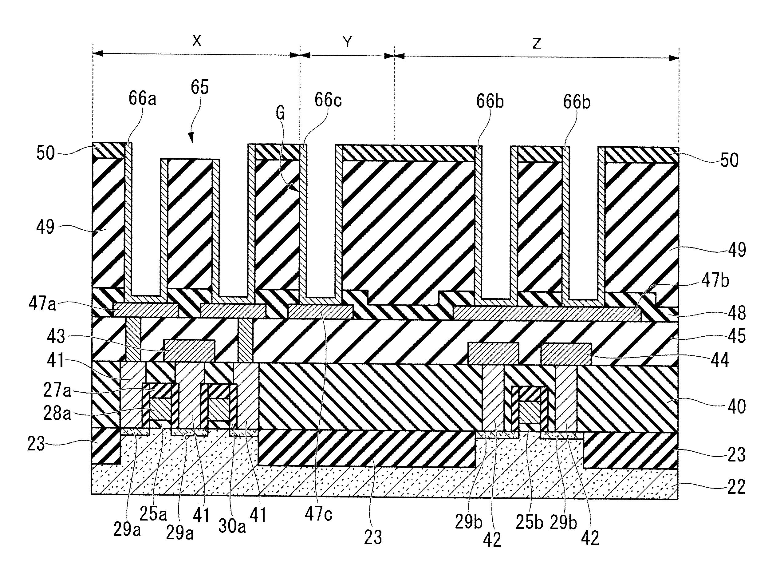
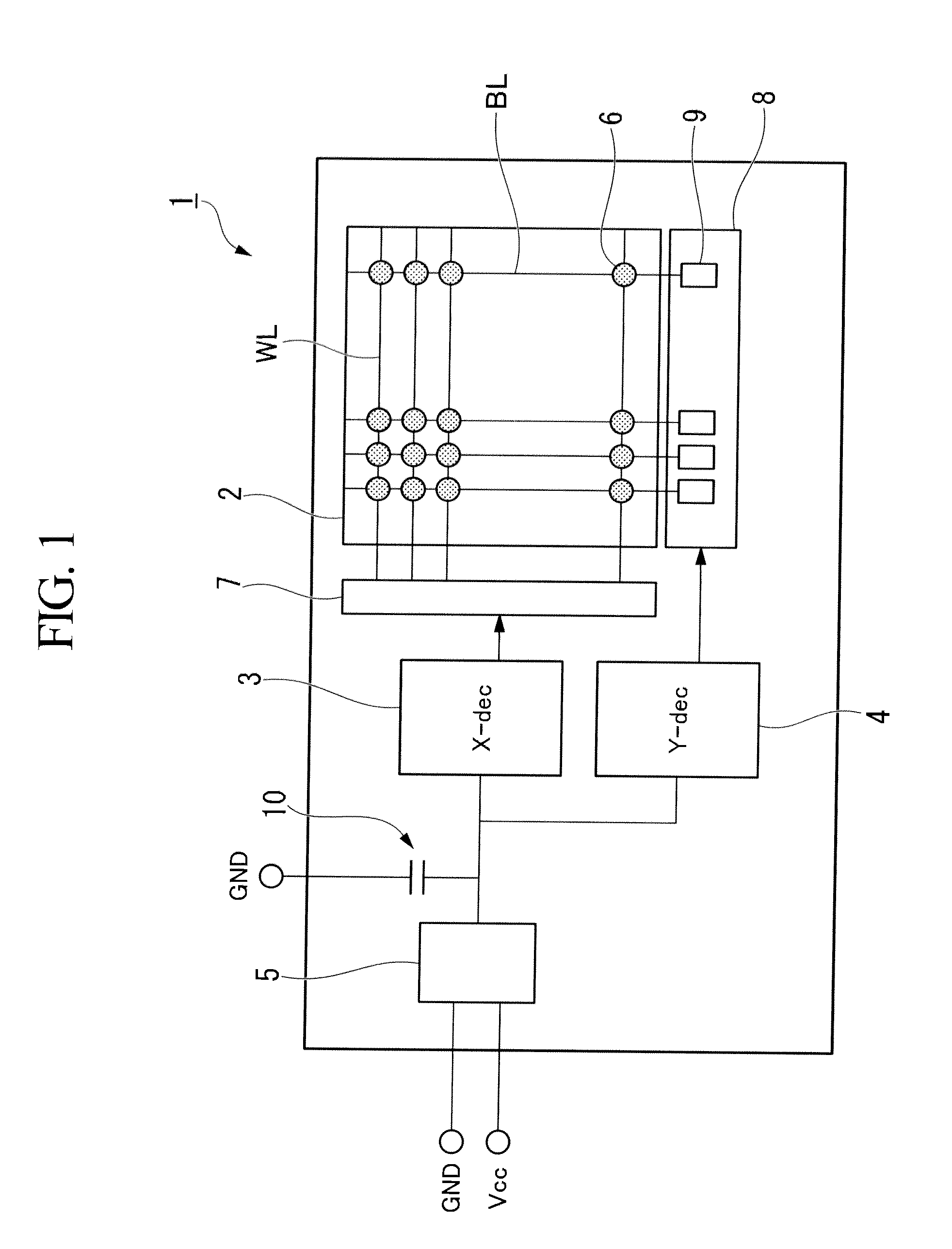
[0034]Hereinafter, a DRAM (Dynamic Random Access Memory), which is a semiconductor device of a first embodiment of the present invention, is explained. FIG. 1 is a circuit diagram illustrating main part of the DRAM including a decoder circuit.

[0035]As shown in FIG. 1, a semiconductor chip 1 of the DRAM includes: a memory cell array 2; an X-decoder 3; a Y-decoder 4; and an internal power-supply circuit 5 that supplies an internal power to the decoders 3 and 4.

[0036]The memory cell array 2 includes multiple word wires WL and multiple bit wires BL. A memory cell 6 is formed at an intersection of each word wire WL with each bit wire BL. The memory cell 6 includes a capacitor 21a for storing data (see FIG. 3), and an MOS transistor for performing selection.

[0037]An external power-supply voltage Vcc and a ground voltage GND, which are supplied from outside the semiconductor chip 1, are supplied to an internal power-supply circuit 5. Then, the external power-supply voltage Vcc and the grou...

second embodiment

[0118]Hereinafter, a semiconductor device according to a second embodiment of the present invention is explained with reference to FIG. 18. The second embodiment is a modification of the first embodiment, and differs from the first embodiment only in the structure of a compensation capacitor. Therefore, like reference numerals denote like elements between the first and second embodiments, and explanations of elements other than the compensation capacitor are omitted appropriately.

[0119]As shown in FIG. 18, a compensation capacitor 90 of the second embodiment has a structure in which multiple blocks are connected in series where the compensation capacitor 10 of the first embodiment is regarded as one block. Specifically, the compensation capacitor element 90 includes a compensation capacitor 10a in a first block B1 and a compensation capacitor 10b in a second block B2.

[0120]The upper electrode 69b, which is included in the compensation capacitor 90, is provided for each of the first ...

third embodiment

[0125]Hereinafter, a semiconductor device according to a third embodiment of the present invention is explained with reference to FIG. 19. The third embodiment is a modification of the second embodiment. Like reference numerals denote like elements between the second and third embodiments.

[0126]A compensation capacitor 91 of the third embodiment differs from the compensation capacitor 90 of the second embodiment in that the pad 47b is formed for each of a compensation capacitor element 10c in the first block B1 and a compensation capacitor element 10d in the second block B2, and one upper electrode 69d connects lower electrodes in the first and second blocks B1 and B2. In other words, the upper electrode 69d in the first block is electrically connected to the upper electrode 69d in the second block.

[0127]In this case, a set of the pad 47b, a drawing wire 84, and a contact plug 85 is provided for each of the first and second blocks B1 and B2. The pad 47b in one block is connected to ...


PUM


Abstract

A semiconductor device may include, but is not limited to: a semiconductor substrate; a memory capacitor; and a first compensation capacitor. The semiconductor substrate has at least first and second regions. The memory capacitor is positioned over the first region. The memory capacitor may include, but is not limited to: a first lower electrode; and a first dielectric film covering inner and outer surfaces of the first lower electrode. The first compensation capacitor is positioned over the second region. The first compensation capacitor includes, but is not limited to: a second lower electrode; a second dielectric film covering an inner surface of the second lower electrode; and a first insulating film covering an outer surface of the second lower electrode.

Description

BACKGROUND OF THE INVENTION[0001]1. Field of the Invention[0002]The present invention relates to a semiconductor device.[0003]Priority is claimed on Japanese Patent Application No. 2010-103858, filed Apr. 28, 2010, the content of which is incorporated herein by reference.[0004]2. Description of the Related Art[0005]Generally, regarding semiconductor devices, such as a DRAM, operating power-supply voltages of circuit elements have been lowered to decrease power consumption. Specifically, a power-supply voltage, which is supplied from an external unit, is lowered to a desired value in a semiconductor device, and then is supplied to circuit elements.[0006]Recently, with the decrease in operating power-supply voltages, it has been more and more important to stabilize and supply a power-supply voltage since a variation in power-supply voltage greatly affects circuit operation. For this reason, a technique of providing a compensation capacitor between a wire for supplying a power-supply v...

Claims


Application Information

Patent Timeline
Patent Type & Authority Applications(United States)
IPC IPC(8): H01L29/92H01L27/06
CPCH01L27/10817H01L27/10852H01L28/91H01L27/10897H01L27/10894H10B12/318H10B12/50H10B12/09H10B12/033
Inventor NAKAMURA, YOSHITAKAYAMAZAKI, YASUSHI
Owner LONGITUDE LICENSING LTD
Why Eureka
Try Eureka