A method of manufacturing a mems capacitor microphone, a stack of foils comprising such a mems capacitor microphone, an electronic device comprising such a mems capacitor microphone and use of the ele

A technology of microsystems and electrodes, applied in the manufacture of microsystems, microsystems, foil stacks including microsystems, electronic devices including microsystems, and the use of electronic devices, capable of solving problems such as complex methods

Inactive Publication Date: 2008-09-10
KONINKLIJKE PHILIPS ELECTRONICS NV
View PDF0 Cites 6 Cited by
  • Summary
  • Abstract
  • Description
  • Claims
  • Application Information

AI Technical Summary

Problems solved by technology

[0003] The problem with this known method is that it is a relatively complex method

Method used


Image

  • A method of manufacturing a mems capacitor microphone, a stack of foils comprising such a mems capacitor microphone, an electronic device comprising such a mems capacitor microphone and use of the ele
  • A method of manufacturing a mems capacitor microphone, a stack of foils comprising such a mems capacitor microphone, an electronic device comprising such a mems capacitor microphone and use of the ele
  • A method of manufacturing a mems capacitor microphone, a stack of foils comprising such a mems capacitor microphone, an electronic device comprising such a mems capacitor microphone and use of the ele

Examples


Embodiment Construction

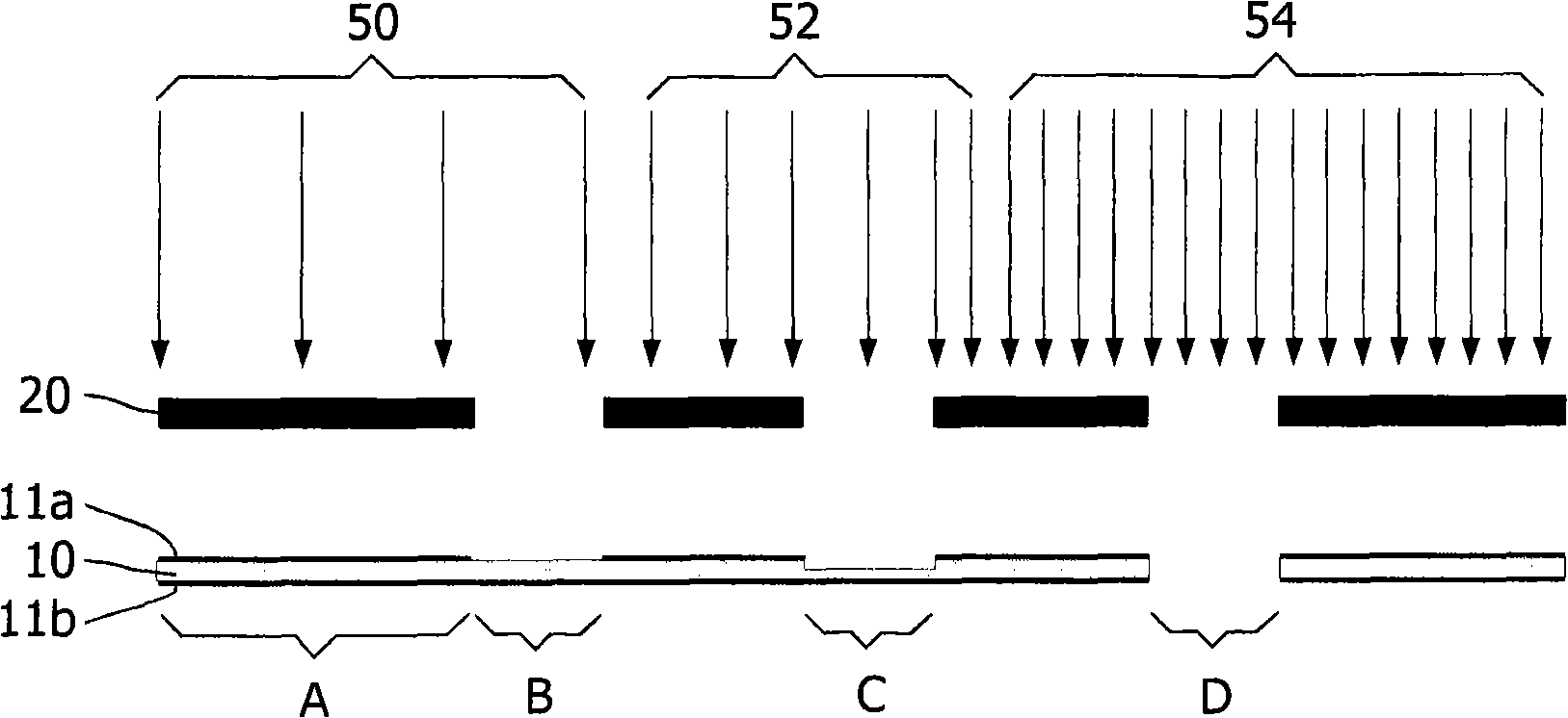
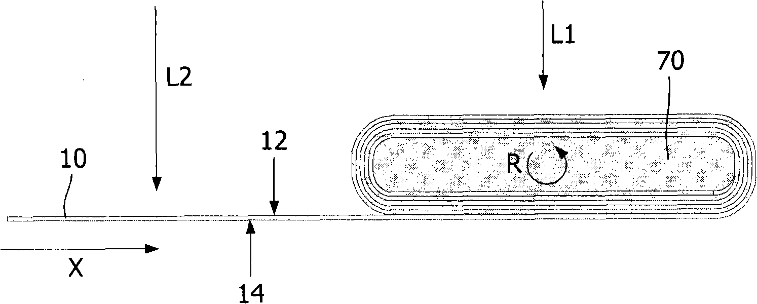
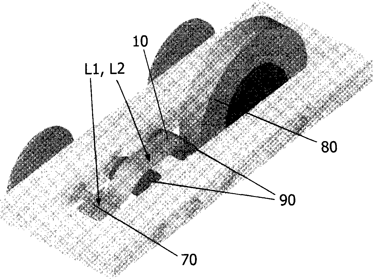
[0092] Hereinafter, a detailed description of the present invention will be given. As stated above, the present invention relates to methods of manufacturing microsystems as well as to such microsystems themselves. Many embodiments of the microsystem according to the invention are possible, and these embodiments are varied. However, all of these embodiments have one common factor in that they consist of joined-together laminates of pre-processed electrically insulating foils having, on at least one side thereof, conductive layer.

[0093] The method of manufacturing the microsystem includes the following sub-steps:

[0094] - applying a conductive layer on at least one side of the foil (so both sides are also possible, and in some cases even preferably on both sides);

[0095] - pretreating said foil;

[0096] - laminating said foils, thereby forming a microsystem;

[0097] - bonding (bonding, joining) said foil; and

[0098] - Separation of the microsystem from said foi...


PUM

PropertyMeasurementUnit
thicknessaaaaaaaaaa

Abstract

The invention relates to a method of manufacturing a microsystem and further to such microsystem. With the method a microsystem can be manufactured by stacking pre-processed foils (10) having a conductive layer (lla, llb) on at least one side. After stacking, the foils (10) are sealed, using pressure and heat. Finally the microsystems are separated from the stack (S). The pre-processing of the foils (preferably done by means of a laser beam) comprises a selection of the following steps: (A) leaving the foil intact, (B) locally removing the conductive layer, (C) removing the conductive layer and partially evaporating the foil (10), and (D) removing both the conductive layer as well as foil (10), thus making holes in the foil (10). In combination with said stacking, it is possible to create cavities, freely suspended cantilevers and membranes. This opens up the possibility of manufacturing various microsystems, like MEMS devices and microfluidic systems.

Description

technical field [0001] The invention relates to a method of manufacturing a microsystem with spaces. The invention also relates to such a microsystem. The invention also relates to a stack of foils comprising such a microsystem according to the invention. The invention also relates to an electronic device comprising a microsystem according to the invention. The invention also relates to the use of such an electronic device. Background technique [0002] The above method and microsystem are disclosed in the article "Fabrication, Assembly, and Testing of RF MEMS Capacitive Switches" published by Ramadoss, R., etc. in IEEE Transactions on Advanced Packaging, Volume 26, No. 3, August 2003, pages 248-254 Using Flexible Printed Circuit Technology". In this known method, an overclad copper substrate layer is provided. Polish the copper cladding to make it more planar. Thereafter, coplanar waveguides are defined in the copper cladding using photolithography and etching steps. ...

Claims


Application Information

Patent Timeline
Patent Type & Authority Applications(China)
IPC IPC(8): B81C1/00B81C99/00
CPCB81C2201/019F16K99/0001Y10T428/24851B01L2300/0627B01L3/502707F16K99/0051F04B43/043B01L2300/123B81C1/00119B01L2400/0638B81C1/00182B01L2300/0819F16K99/0007B81C99/0095F16K99/0015B01L2200/12B01L2300/1827B01L3/502738F16K2099/008F16K99/0034B01L2200/10B01L2300/0887F16K2099/0084H01L29/00B81C1/00
Inventor G·兰格赖斯J·W·威坎普J·B·吉斯伯斯
Owner KONINKLIJKE PHILIPS ELECTRONICS NV
Why Eureka
Try Eureka