

Solid-state imaging device, drive method thereof and camera system
- Summary
- Abstract
- Description
- Claims
- Application Information
AI Technical Summary
Benefits of technology
Problems solved by technology
Method used
Image

Examples
Embodiment Construction
sensor including four transistors according to the embodiment;
[0031]FIG. 4 is a circuit diagram showing a specific configuration example of each load element unit of the current source circuit according to the embodiment;
[0032]FIG. 5 is a view showing state transition from the turning on of a selection transistor of the pixel until a vertical signal line becomes a settlement level;
[0033]FIG. 6 is a circuit diagram showing another specific configuration example of each load element unit of the current source circuit according to the embodiment; and
[0034]FIG. 7 is a view showing an example of a configuration of a camera system to which the solid-state imaging device according to an embodiment of the invention is applied.
DESCRIPTION OF THE PREFERRED EMBODIMENTS
[0035]Hereinafter, embodiments of the invention will be explained with reference to the drawings.
[0036]The explanation will be made in the following order.
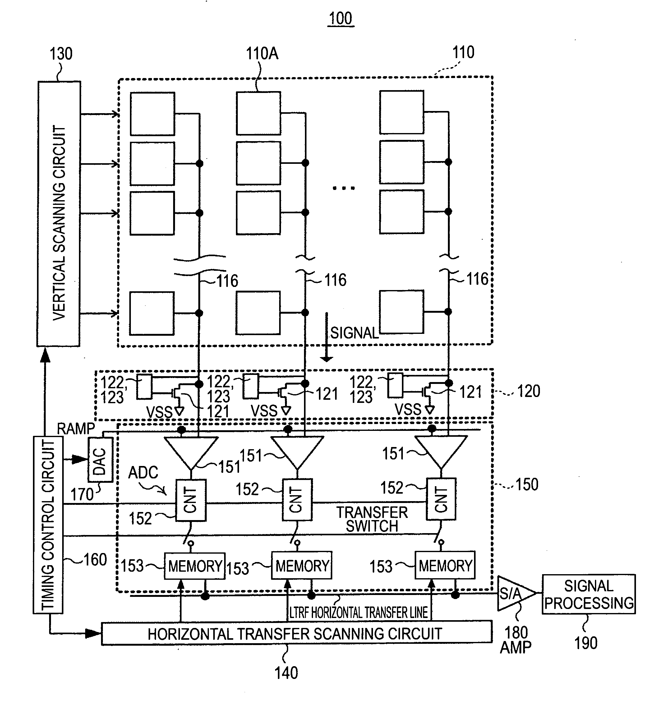
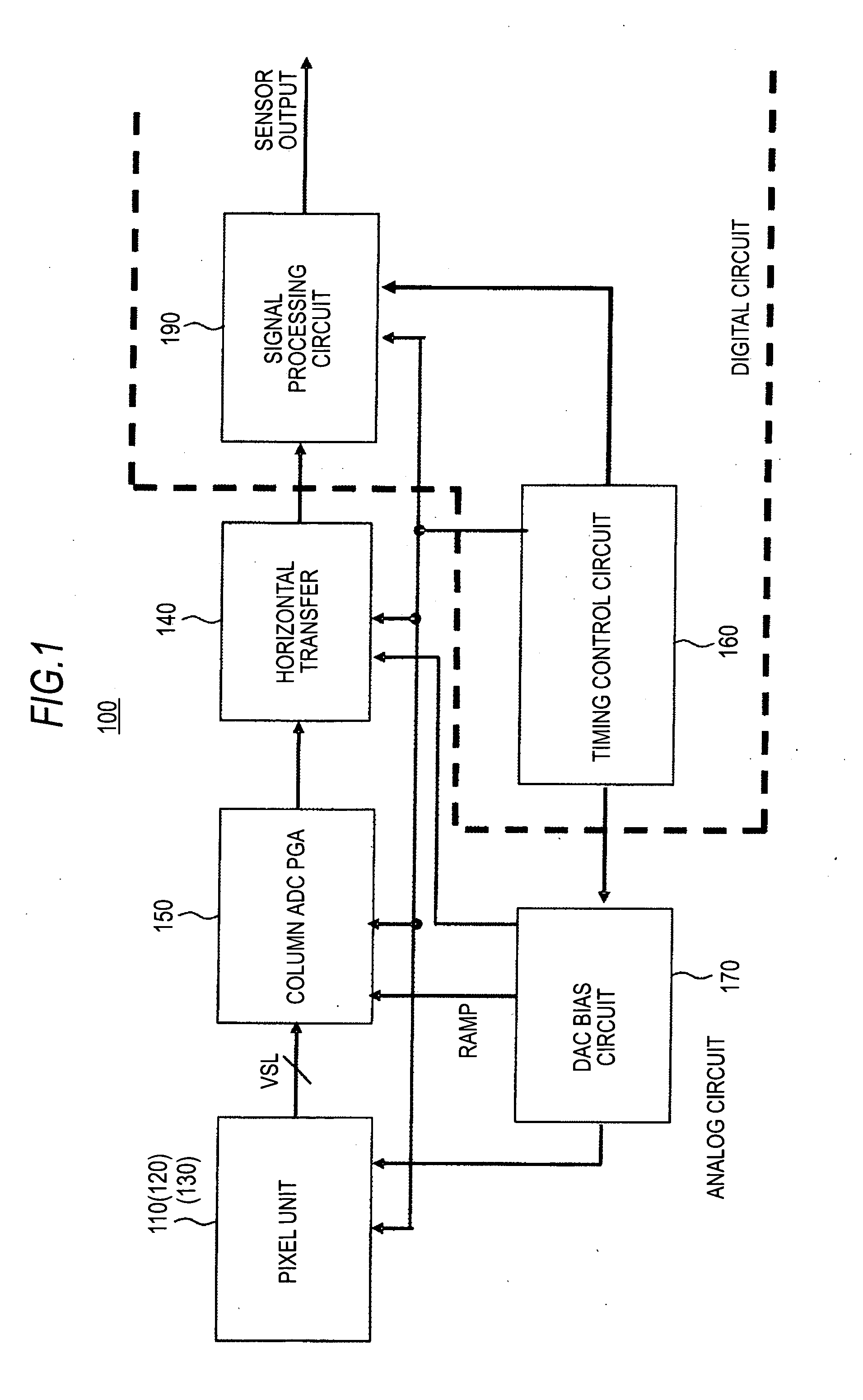
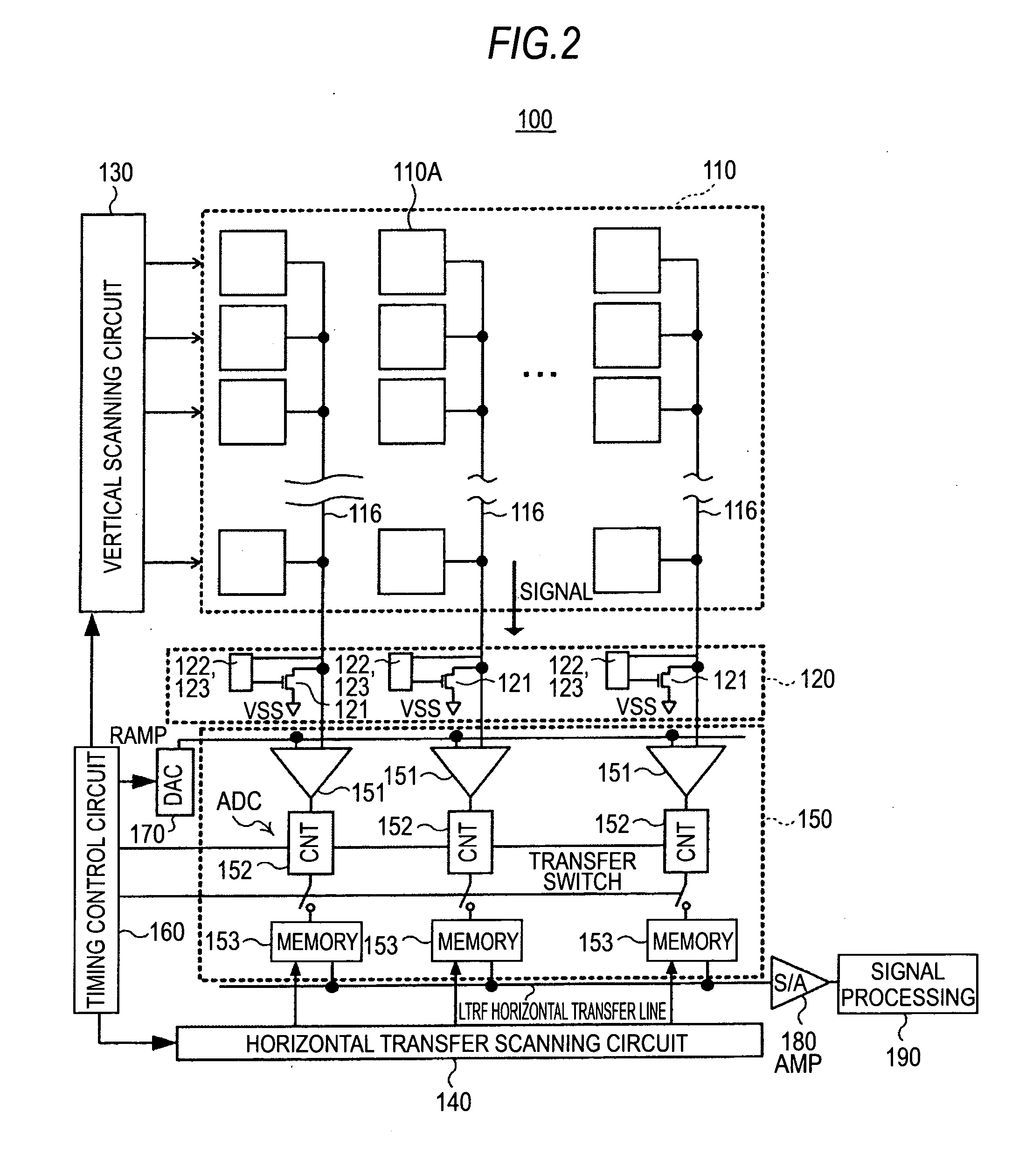
[0037]1. Outline of the entire configuration of a solid-state imaging devi...
PUM
 Abstract
Description
Claims
Application Information