Wafer processing method

Active Publication Date: 2011-11-24
DISCO CORP
View PDF1 Cites 17 Cited by
  • Summary
  • Abstract
  • Description
  • Claims
  • Application Information

AI Technical Summary

Benefits of technology

[0011]According to the present invention, although the reinforcing plate is formed from only the heat-resistant bond, the back side of the wafer is ground so as to leave the annular reinforcing portion in the outer circumferential portion of the wafer in the back grinding step, so that the strength of the wafer is maintained by the annular

Problems solved by technology

Accordingly, it is difficult to remove the reinforcing plate from the f

Method used


Image

  • Wafer processing method
  • Wafer processing method
  • Wafer processing method

Examples


Example

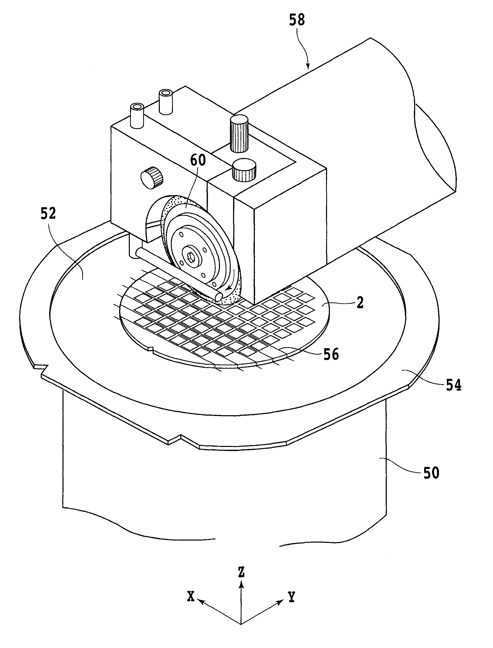
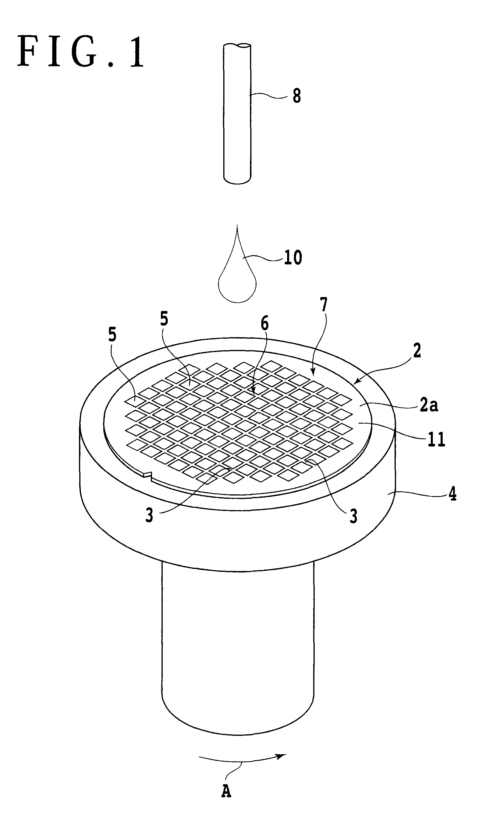
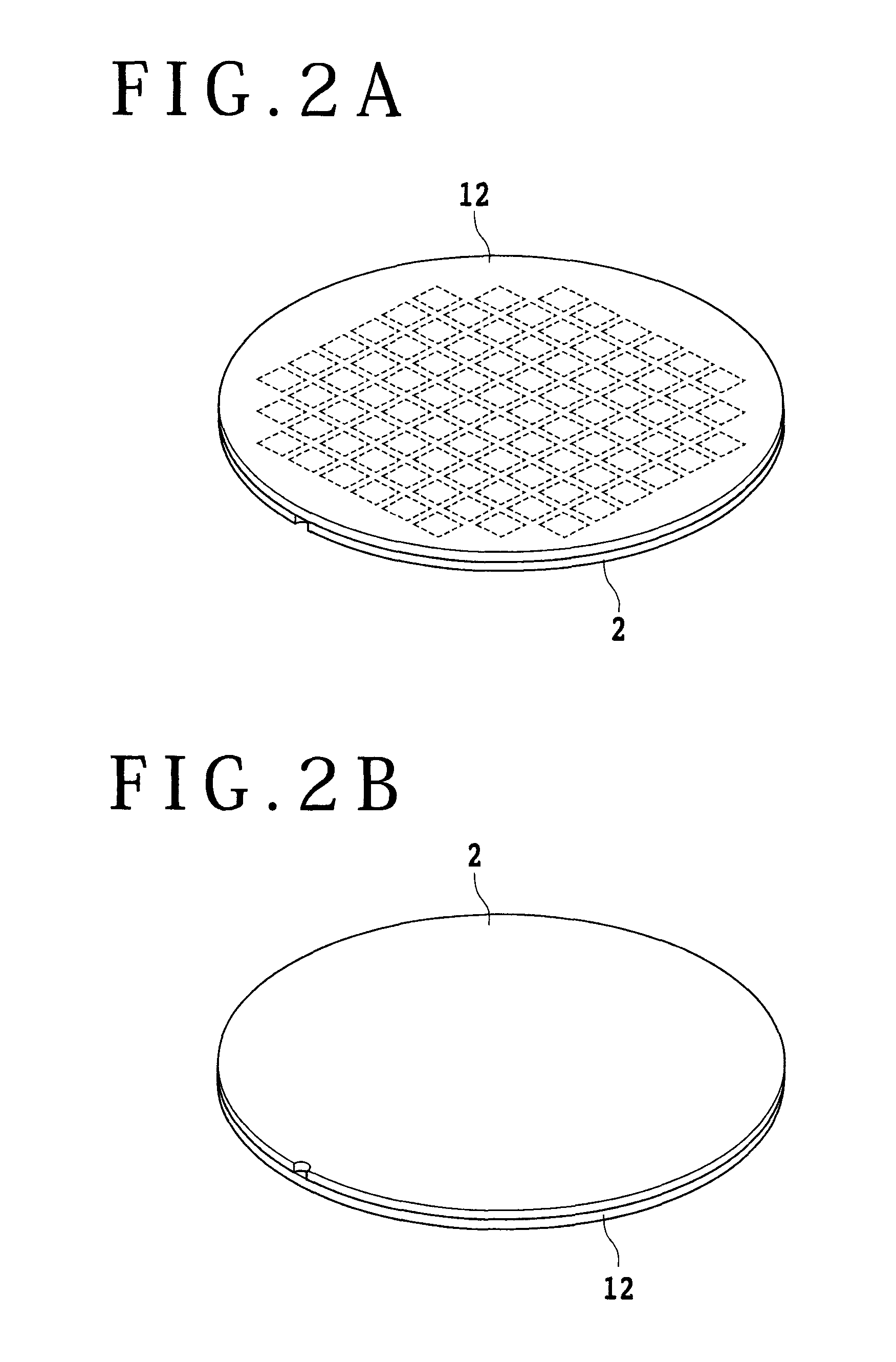
[0022]A preferred embodiment of the present invention will now be described in detail with reference to the drawings. Referring to FIG. 1, there is shown a perspective view for illustrating a heat-resistant bond supplying step. In this preferred embodiment, a heat-resistant bond 10 is supplied to the front side 2a of a semiconductor wafer (which will be hereinafter referred to simply as wafer) 2 by spin coating. First, the wafer 2 is held under suction on a rotatable chuck table 4. A plurality of crossing streets (division lines) 3 are formed on the front side 2a of the wafer 2 to partition a plurality of regions where a plurality of devices 5 such as ICs and LSIs are respectively formed. The wafer 2 has a device area 6 where the plural devices 5 are formed on the front side 2a and a peripheral marginal area 7 surrounding the device area 6.

[0023]The heat-resistant bond 10 is supplied to the front side 2a of the wafer 2 by spin coating in such a manner that the chuck table 4 is rotat...


PUM


Abstract

A processing method for a wafer having a device area where a plurality of devices are formed on the front side of the wafer and a peripheral marginal area surrounding the device area. The processing method includes a reinforcing plate forming step of applying a heat-resistant bond to the front side of the wafer and solidifying the heat-resistant bond to thereby form a reinforcing plate from only the heat-resistant bond, a back grinding step of holding the reinforcing plate on a chuck table and grinding the back side of the wafer in the device area to thereby form a circular recess in the device area and leave an annular reinforcing portion in the peripheral marginal area, a through electrode forming step of forming a through electrode connected to an electrode of each device formed on the front side of the wafer, from the back side of the wafer fixed to the reinforcing plate, and a reinforcing plate removing step of supplying a solvent for dissolving the heat-resistant bond to the reinforcing plate, thereby removing the reinforcing plate.

Description

BACKGROUND OF THE INVENTION[0001]1. Field of the Invention[0002]The present invention relates to a wafer processing method including the steps of grinding the back side of a wafer and next forming a through electrode connected to an electrode of each device formed on the front side of the wafer from the back side of the wafer.[0003]2. Description of the Related Art[0004]A plurality of devices such as ICs and LSIs are formed on the front side of a semiconductor wafer so as to be partitioned by a plurality of crossing division lines. The semiconductor wafer is divided into the individual devices by a dicing apparatus, and these devices divided from each other are widely used in various electrical equipment such as a mobile phone and a personal computer.[0005]In recent semiconductor device technology, a stacked semiconductor package such that a plurality of semiconductor chips are stacked is effectively used in achieving a higher density and a reduction in size and thickness. In this s...

Claims


Application Information

Patent Timeline
IPC IPC(8): H01L21/78
CPCH01L21/304H01L21/78H01L21/67092
Inventor KOBAYASHI, YOSHIKAZU
Owner DISCO CORP
Why Eureka
Try Eureka