Semiconductor wafer structure and multi-chip stack structure

a technology of multi-chip stack and semiconductor wafer, which is applied in the direction of semiconductor devices, semiconductor/solid-state device details, electrical apparatus, etc., can solve the problems of deformation and cracks in the 3-d multi-chip stack structure, further yield losses in the 3-d multi-chip stack package structure and 3c electronic products, and achieve the effect of enhancing the reliability of the multi-chip stack package structure and minimizing the problem of misalignmen

Inactive Publication Date: 2011-12-01
CHIPMOS TECH INC
View PDF2 Cites 22 Cited by
  • Summary
  • Abstract
  • Description
  • Claims
  • Application Information

AI Technical Summary

Benefits of technology

In order to minimize the misalignment problem between metal electrodes and the CTE mismatch issue between different materials and thus to enhance the reliability of the multi-chip stack package structures, the objective of the present invention is to provide a semiconductor wafer structure with some kinds of through-silicon-via electrode structures.

Problems solved by technology

During the wafer-to-wafer stacking process, destructive deformations and cracks may occur in the 3-D multi-chip stacked structures due to factors such as alignment error between the metal electrodes and CTE mismatch between different materials of silicon, insulating materials and metals.
As shown in FIG. 10, the CTE mismatch may induce potential joint breakage and deformations in x-y-z directions, especially along the Z-axis, at the interfaces between the bonded copper electrodes as well as cracks in silicon, leading to reliability issues of the multi-wafer / multi-chip stack structures with further yield losses in the 3-D multi-chip stack package structures and 3C electronic products.

Method used


Image

  • Semiconductor wafer structure and multi-chip stack structure
  • Semiconductor wafer structure and multi-chip stack structure
  • Semiconductor wafer structure and multi-chip stack structure

Examples


first embodiment

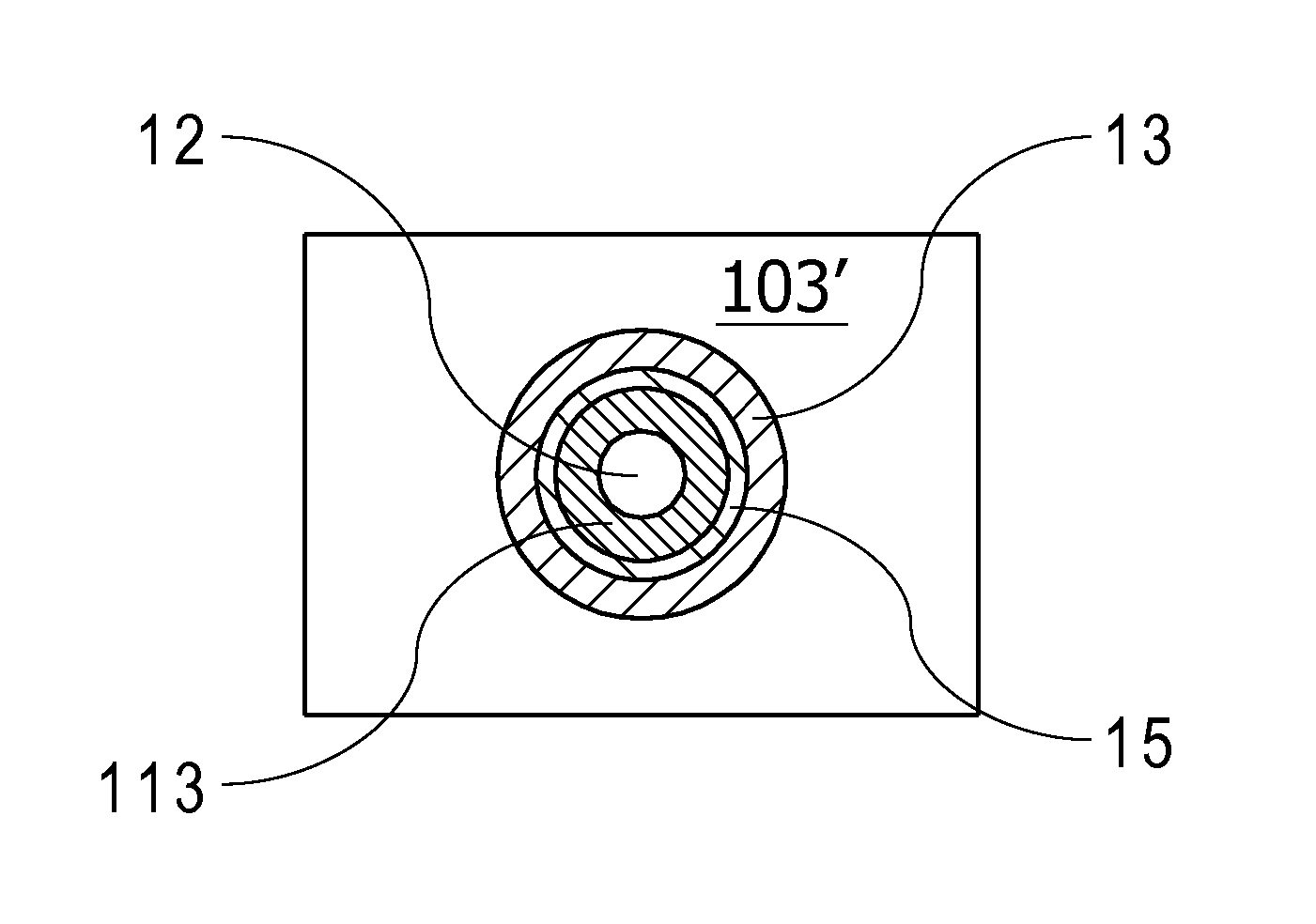
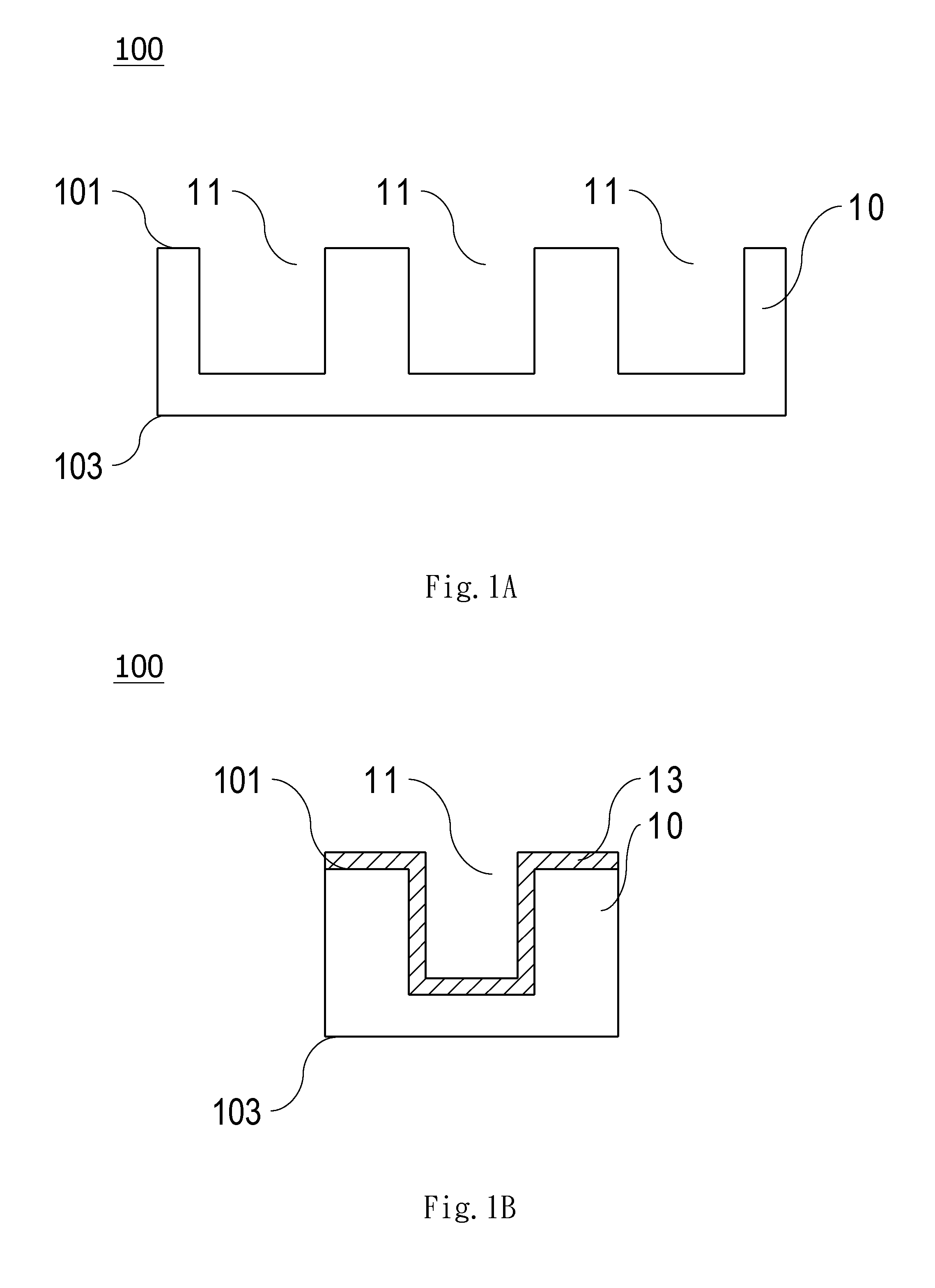
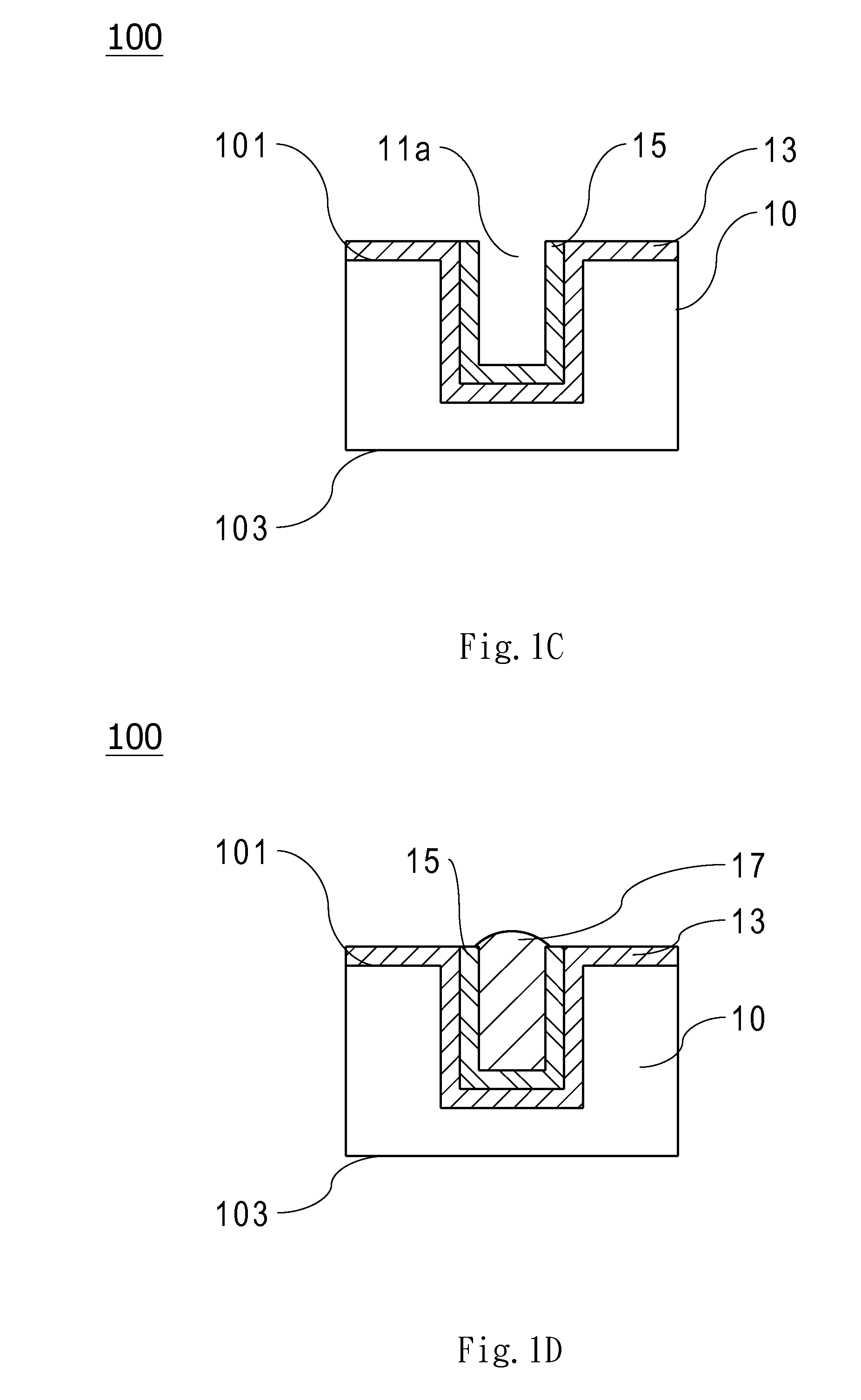
As shown in FIG. 4A, the present invention provides multi-chip stack structure that is formed by vertically stacking a plurality of semiconductor chips with through-silicon-via electrode structures of FIG. 2A. Please also refer to FIGS. 1B, 1C and 1F. Each of the plurality of semiconductor chips has a first surface 101, a second surface 103′ opposite to the first surface 101 and a plurality of through-silicon holes 11 formed therein. The plurality of through-silicon holes 11 connect the first surface 101 and the second surface 103′. A through-silicon-via electrode structure is formed in each of the plurality of through-silicon holes 11, and the through-silicon-via electrode structure comprises a dielectric layer 13 formed on an inner wall of the through-silicon hole 11, a barrier layer 15 formed on an inner wall of the dielectric layer 13 and defining a vacancy 11a therein, a filling metal layer 17 filled into the vacancy 11a and having a first end 171 and a second end 173 opposite ...

second embodiment

Next, as shown in FIG. 4B, the present invention provides multi-chip stack structure which is formed by vertically stacking a plurality of semiconductor chips with through-silicon-via electrode structures of FIG. 2B. In this embodiment, each of the structures on the first surface 101 of the semiconductor chip in FIG. 2B is identical to that in FIG. 2A; the difference is that a soft metal cap 111 is further formed on the second end 173 of each of the plurality of filling metal layers 17 near the lapped second surface 103′ of the semiconductor chip in FIG. 2A. In this embodiment, the horizontal dimension of the soft metal cap 111 is identical to that of the filling metal layer 17. Thus, the multi-chip stack structure is formed by connecting the plurality of soft metal caps 19a / 19b of one of the plurality of semiconductor chips to the plurality of soft metal caps 111 of another semiconductor chip.

third embodiment

Next, as shown in FIG. 4C, the present invention provides multi-chip stack structure which is formed by vertically stacking a plurality of semiconductor chips with through-silicon-via electrode structures of FIG. 2C. In this embodiment, similar to the semiconductor chip in FIG. 2B, soft metal caps 111 are formed on the second ends 173 of the plurality of filling metal layers 17, but the horizontal dimension of the soft metal cap 111 is larger than that of the filling metal layer 17 so that the soft metal cap 111 overlays the barrier layer 15 and even a portion of the dielectric layer 13′. Thus, the multi-chip stack structure is formed by connecting the plurality of soft metal caps 19a / 19b of one of the plurality of semiconductor chips to the plurality of soft metal caps 111 of another semiconductor chip.


PUM


Abstract

A semiconductor wafer structure comprises a first surface and a second surface opposite to the first surface, a plurality of chip areas formed on the first surface, a plurality of through-silicon holes formed in each of the plurality of chip areas connecting the first surface and the second surface, and a through-silicon-via (TSV) electrode structure formed in each through-silicon hole. Each through-silicon-via electrode structure comprises a dielectric layer formed on the inner wall of the through-silicon hole, a barrier layer formed on the inner wall of the dielectric layer and defining a vacancy therein, a filling metal layer filled into the vacancy, a first end of the filling metal layer being lower than the first surface forming a recess, and a soft metal cap connecting to and overlaying the first end of the filling metal layer, wherein a portion of the soft metal cap is formed in the recess and the soft metal cap protrudes out of the first surface. Hence, the reliability of multi-chip stack package structure can be enhanced with the application of these soft metal caps.

Description

BACKGROUND OF THE INVENTION1. Field of the InventionThe present invention relates to a semiconductor wafer or chip with through-silicon-via electrode structures, and more particularly to a multi-chip stack structure with through-silicon-via electrode structures.2. Description of the Prior ArtAs the trend of designing consumer electronic products leans to meet strong demands for light weight, thinness, and slightness, the integrated circuit manufacturing technologies must keep advancing; for example, the line widths of integrated circuits are getting narrower and narrower. In addition to the requirements for smaller volume and lighter weight, lower price is another requirement for 3C electronic products to comply with. Therefore, the manufacturing cost of various integrated circuit dice which play important roles in 3C electronic products is also required to be reduced accordingly.To reduce the manufacturing cost of integrated circuit dice, some advanced manufacturers have developed ...

Claims


Application Information

Patent Timeline
Patent Type & Authority Applications(United States)
IPC IPC(8): H01L23/498
CPCH01L21/563H01L2924/0002H01L23/481H01L24/03H01L24/04H01L24/05H01L24/11H01L24/13H01L24/16H01L24/92H01L24/94H01L25/0657H01L2224/0345H01L2224/03462H01L2224/03464H01L2224/0401H01L2224/05009H01L2224/0557H01L2224/05655H01L2224/05666H01L2224/06181H01L2224/11462H01L2224/11464H01L2224/13022H01L2224/13025H01L2224/13111H01L2224/13144H01L2224/13155H01L2224/1319H01L2224/1403H01L2224/14181H01L2224/16145H01L2224/16146H01L2224/73204H01L2224/81193H01L2224/92125H01L2224/94H01L2225/06513H01L2225/06544H01L2924/01019H01L21/76898H01L2924/1461H01L2224/9202H01L2924/00H01L2224/05552H01L2924/14
Inventor WANG, DAVID WEILIU, AN-HONGHUANG, HSIANG-MINGLEE, YI-CHANG
Owner CHIPMOS TECH INC
Why Eureka
Try Eureka