Replacement gate mosfet with self-aligned diffusion contact

a diffusion contact and gate mosfet technology, applied in the field of metal oxidesemiconductor field effect transistors, can solve the problems of increasing the probability of electrical interference, and challenging contact structure formation to source and drain regions of field effect transistors

Active Publication Date: 2011-12-08
GLOBALFOUNDRIES US INC
View PDF1 Cites 71 Cited by
  • Summary
  • Abstract
  • Description
  • Claims
  • Application Information

AI Technical Summary

Problems solved by technology

As semiconductor devices shrink in each generation of semiconductor technology, formation of contact structures to source and drain regions of a field effect transistor become challenging because such contact structures not only need to provide reliable electrical contact to the source and drain regions, but also need to avoid electrically shorting to other components such as the gate electrode of the field effect transistor.
Since the etch chemistry employed for the anisotropic etch process remains the same while the lateral dimension of the dielectric gate spacer shrinks with the scaling of semiconductor devices, the likelihood of excessive removal of the dielectric gate spacer within the normal range of process variations during the anisotropic etch increases as the dielectric gate spacer becomes thinner in each technology generation.
Excessive removal of the dielectric gate spacer increases the probability of an electrical short between a contact to the source region or the drain region of a field effect transistor and the gate electrode of the field effect transistor.
Thus, the possibility of excessively thinning the dielectric gate spacer during the anisotropic etch for forming contact vias is a significant concern for product yield and reliability purposes.

Method used


Image

  • Replacement gate mosfet with self-aligned diffusion contact
  • Replacement gate mosfet with self-aligned diffusion contact
  • Replacement gate mosfet with self-aligned diffusion contact

Examples


Embodiment Construction

[0025]As stated above, the present invention relates to a metal-oxide-semiconductor field effect transistor (MOSFET) having at least one self-aligned diffusion contact and methods of manufacturing the same, which are now described in detail with accompanying figures. It is noted that like and corresponding elements mentioned herein and illustrated in the drawings are referred to by like reference numerals.

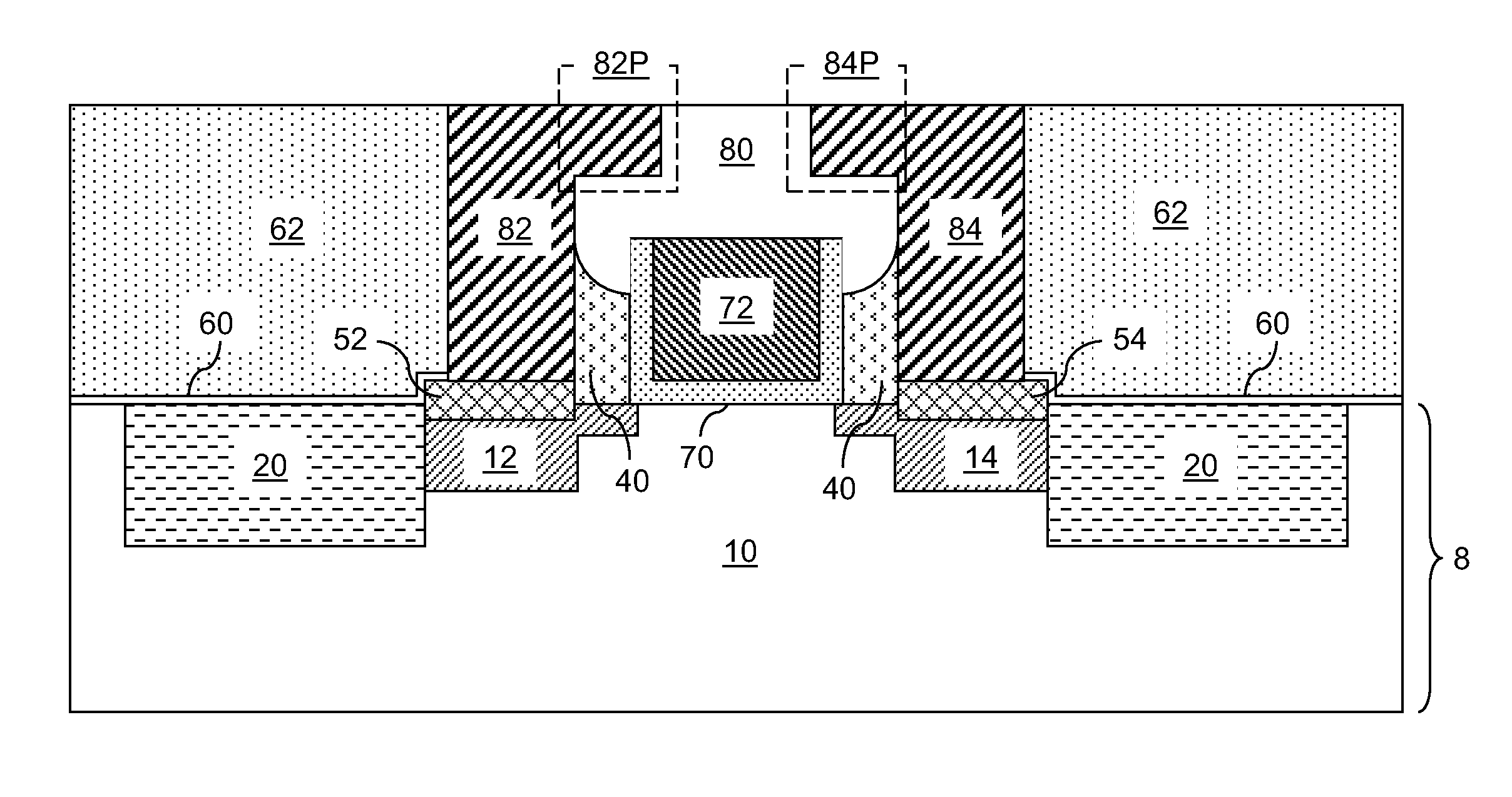
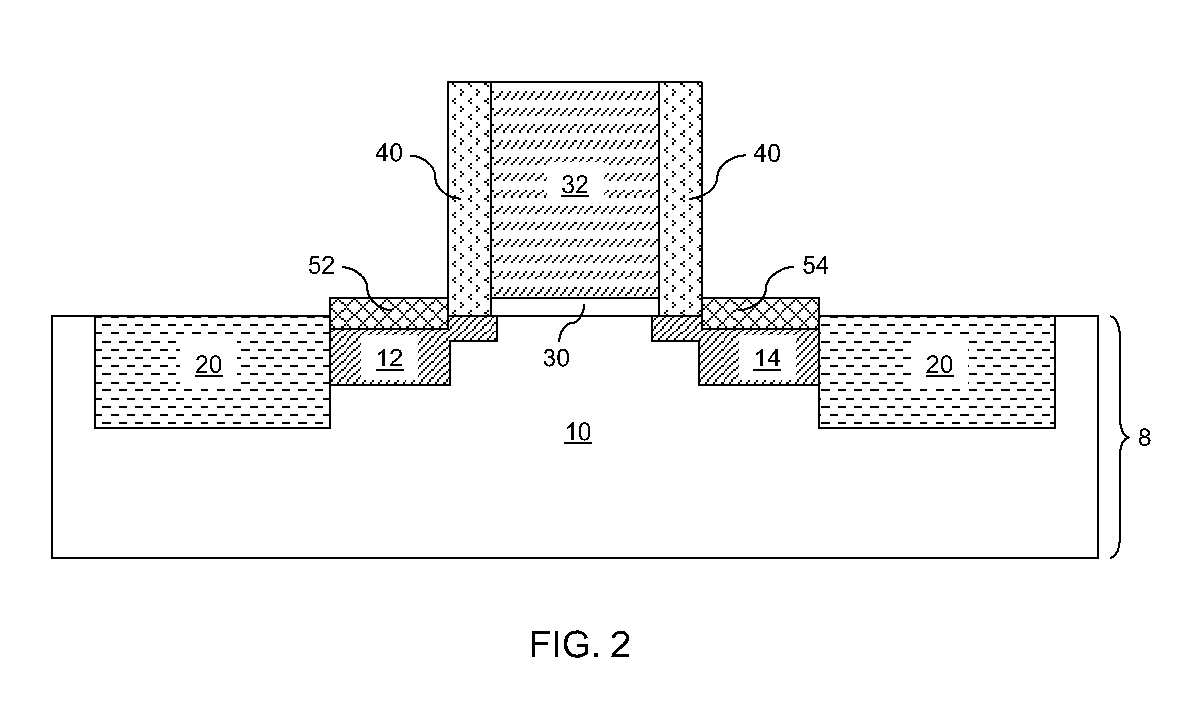
[0026]Referring to FIG. 1, a first exemplary semiconductor structure according to a first embodiment of the present invention includes a semiconductor substrate 8. The semiconductor substrate 8 includes a semiconductor layer 10 and isolation structures 20 embedded in the semiconductor layer 10. The isolation structures 20 include a dielectric material such as silicon oxide and / or silicon nitride. For example, the isolation structures 20 can be shallow trench isolation structures known in the art.

[0027]The semiconductor layer 10 is composed of a semiconductor material such as silico...


PUM


Abstract

A replacement gate field effect transistor includes at least one self-aligned contact that overlies a portion of a dielectric gate cap. A replacement gate stack is formed in a cavity formed by removal of a disposable gate stack. The replacement gate stack is subsequently recessed, and a dielectric gate cap having sidewalls that are vertically coincident with outer sidewalls of the gate spacer is formed by filling the recess over the replacement gate stack. An anisotropic etch removes the dielectric material of the planarization layer selective to the material of the dielectric gate cap, thereby forming at least one via cavity having sidewalls that coincide with a portion of the sidewalls of the gate spacer. A portion of each diffusion contact formed by filling the at least one via cavity overlies a portion of the gate spacer and protrudes into the dielectric gate cap.

Description

BACKGROUND[0001]The present invention relates to semiconductor structures, and particularly to a metal-oxide-semiconductor field effect transistor (MOSFET) having at least one self-aligned diffusion contact and methods of manufacturing the same.[0002]As semiconductor devices shrink in each generation of semiconductor technology, formation of contact structures to source and drain regions of a field effect transistor become challenging because such contact structures not only need to provide reliable electrical contact to the source and drain regions, but also need to avoid electrically shorting to other components such as the gate electrode of the field effect transistor. Since the etch chemistry employed for the anisotropic etch process remains the same while the lateral dimension of the dielectric gate spacer shrinks with the scaling of semiconductor devices, the likelihood of excessive removal of the dielectric gate spacer within the normal range of process variations during the ...

Claims


Application Information

Patent Timeline
Patent Type & Authority Applications(United States)
IPC IPC(8): H01L29/78H01L21/28
CPCH01L21/76897H01L29/4966H01L29/517H01L29/7833H01L29/6653H01L29/66545H01L29/6659H01L29/665H01L21/76834
Inventor JAIN, SAMEER H.RADENS, CARL J.SIDDIQUI, SHAHABSTRANE, JAY W.
Owner GLOBALFOUNDRIES US INC
Why Eureka
Try Eureka