Four-transistor and five-transistor bjt-cmos asymmetric SRAM cells

Inactive Publication Date: 2011-12-08
ASA GIL
View PDF3 Cites 46 Cited by
  • Summary
  • Abstract
  • Description
  • Claims
  • Application Information

AI Technical Summary

Benefits of technology

[0013]A still further aspect of the present invention is directed to a RAM memory for a chip, comprising a collection of memory cells, each memory cell comprising a retention element and a CMOS transistor, the retention elements being asymmetric and comprising bipolar junction transistors, the retention element operatively engaged to the CMOS transistor

Problems solved by technology

The scale down tendency of the integrated circuit industry is causing an increasing technological barrier.
These integrated circuits increase the man

Method used


Image

  • Four-transistor and five-transistor bjt-cmos asymmetric SRAM cells
  • Four-transistor and five-transistor bjt-cmos asymmetric SRAM cells
  • Four-transistor and five-transistor bjt-cmos asymmetric SRAM cells

Examples


Embodiment Construction

[0026]The following detailed description is of the best currently contemplated modes of carrying out the invention. The description is not to be taken in a limiting sense, but is made merely for the purpose of illustrating the general principles of the invention, since the scope of the invention is best defined by the appended claims.

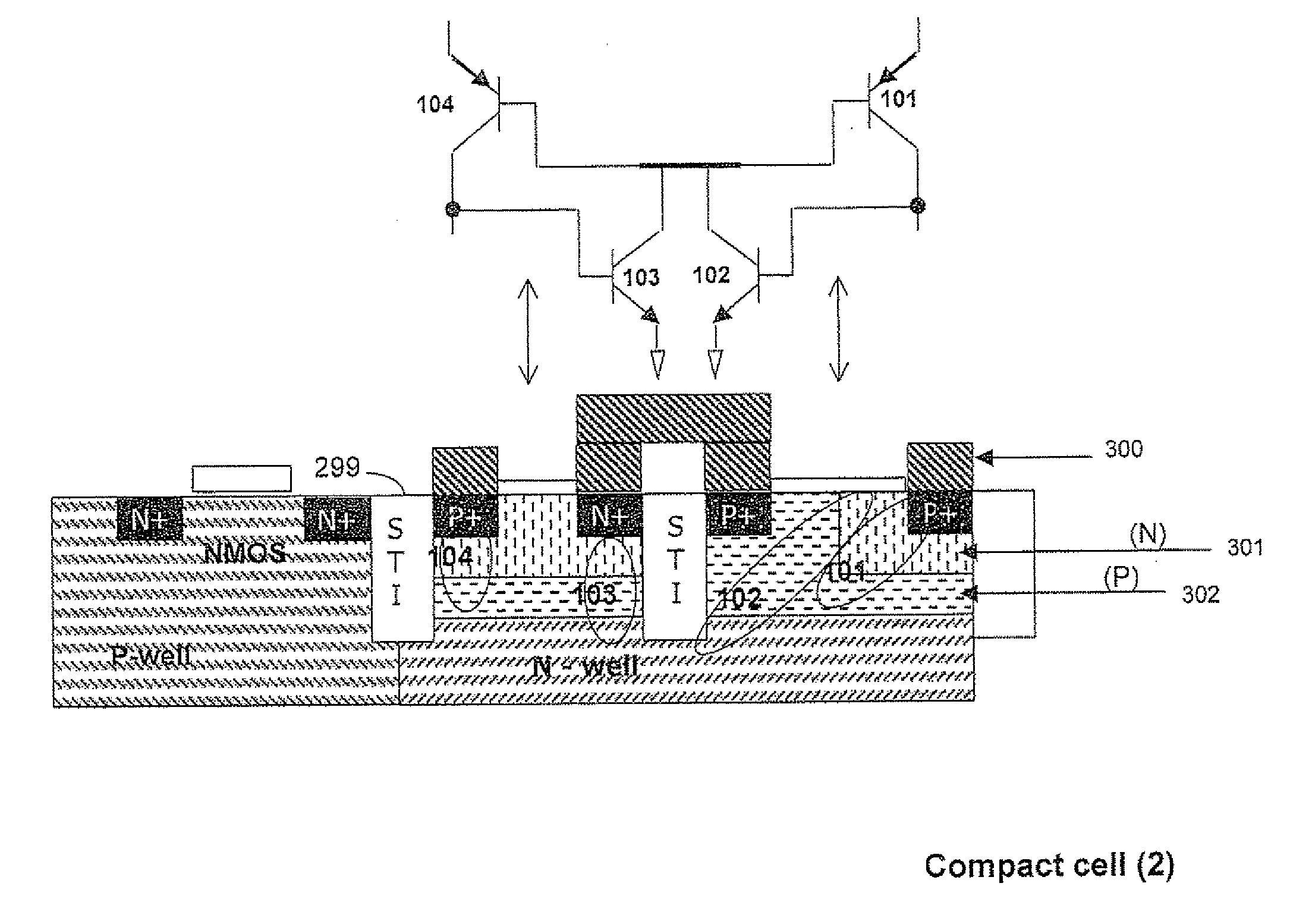
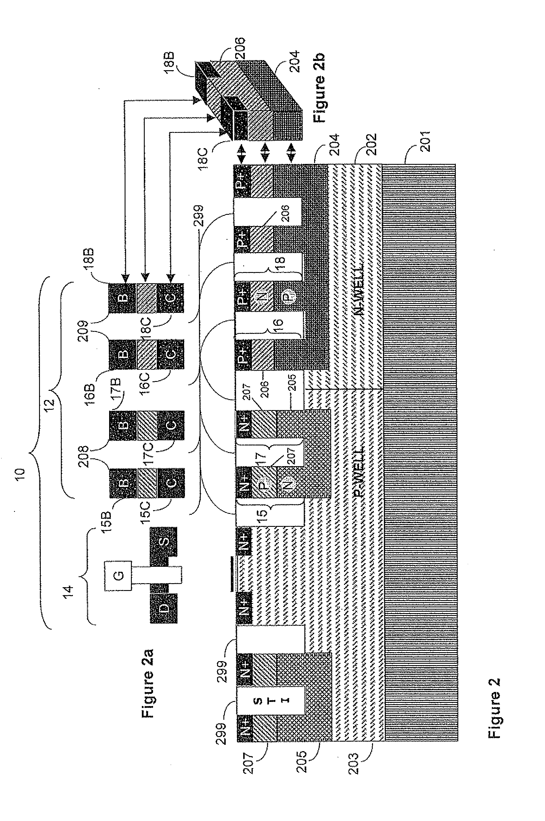
[0027]The present invention generally provides a memory cell for RAM memory and for other volatile memory such as a flip-flop and a register file. The cell may comprise a retention element and either an adjacent NMOS or adjacent PMOS transistor operatively engaged to the retention element. The retention element may be assymetric and may be comprised of four bipolar junction transistors, each of which may be vertically stacked. Other than the retention elements the chip may use CMOS transistors. The NPN bipolar junction transistors may share an N layer and the PNP bipolar junction transistor may share a P layer. For further compactness, in one embodiment...


PUM


Abstract

A memory cell comprises asymmetric retention elements formed of bipolar junction transistors integrated with a CMOS transistor. The BJT transistors of the retention element may be vertically stacked. In one embodiment, the N region of two adjacent NPN BJT transistors may be connected to ground and may form a common emitter of the NPN BJT transistors while the P region of two adjacent PNP BJT transistors may be connected to high voltage and may form a common emitter of the PNP BJT transistors. For further compactness in one embodiment a base of one transistor doubles as a collector of another transistor. The retention element may have only a single bit line and a single write line, with no negative bit line. In some embodiments, a single inverter and only three transistors may form the retention element. Memory space may be cut approximately in half.

Description

PRIORITY INFORMATION[0001]This patent application claims the benefit of and is a continuation-in-part of U.S. Provisional Patent Application No. 61 / 152,704 filed Feb. 15, 2009.FIELD AND BACKGROUND OF THE INVENTION[0002]The present invention relates to memory sells for integrated circuits, and, more particularly to memory cells whose retention elements integrate vertically stacked bipolar transistor transistors (“BJT”) with CMOS transistors.[0003]The scale down tendency of the integrated circuit industry is causing an increasing technological barrier. One of the solutions is three-dimensional integrated circuits. These integrated circuits increase the manufacturing complexity significantly.[0004]FIG. 1A shows an ordinary prior art six-transistor memory cell. As can be seen, it has two complementary bit lines, a bit line and a negative bit line. These two complementary bit lines are also tied to differential sense amplifier that has the ability to speed up the loaded bit lines.[0005]M...

Claims


Application Information

Patent Timeline
IPC IPC(8): G11C11/34
CPCG11C11/411G11C11/412H01L21/8249H01L27/0688H01L27/11H03K3/288H01L27/0623H01L27/1025H10B10/10H10B10/00
Inventor ASA, GIL
Owner ASA GIL
Why Eureka
Try Eureka