Coating method and manufacturing method of organic el display

a technology of organic el display and manufacturing method, which is applied in the direction of coating, solid-state device, chemical vapor deposition coating, etc., can solve problems such as misalignment of coating position

Active Publication Date: 2011-12-08
PANASONIC INTELLECTUAL PROPERTY MANAGEMENT CO LTD
View PDF4 Cites 9 Cited by
  • Summary
  • Abstract
  • Description
  • Claims
  • Application Information

AI Technical Summary

Benefits of technology

[0025]With the coating method of the above embodiments of the present invention, an ink droplet is ejected on a first pixel region and on a first lyophobic portion by the inkjet printing, and ink is ejected on a second pixel region while correcting the timing of ink ejection on the second pixel region based on a deviation of the landing position of the ink droplet on the first lyophobic portion from a set ink landing position. As a result, ink can

Problems solved by technology

Pixel regions to be coated with ink are 40 to 60 um in size; therefore, fail

Method used


Image

  • Coating method and manufacturing method of organic el display
  • Coating method and manufacturing method of organic el display
  • Coating method and manufacturing method of organic el display

Examples


embodiment 1

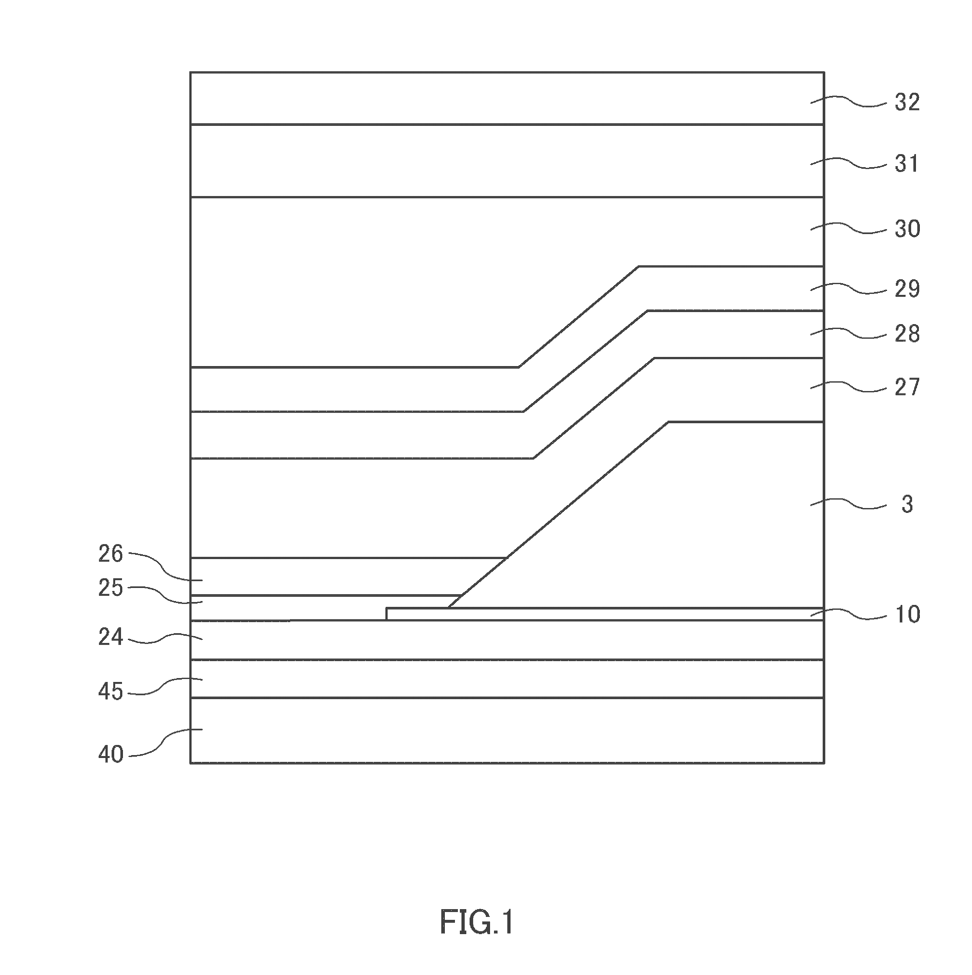
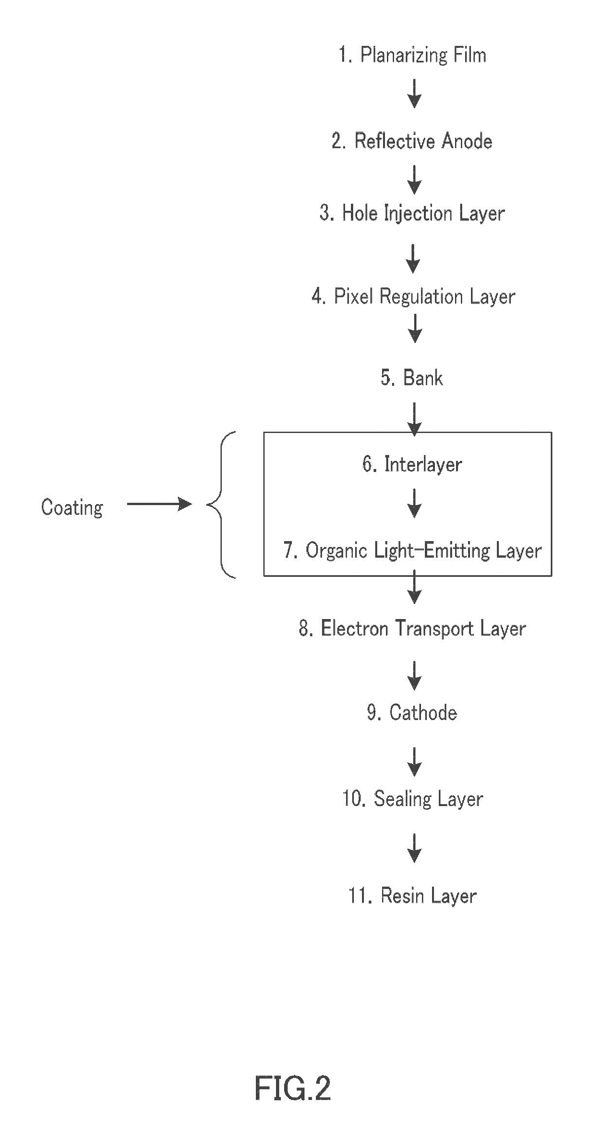
[0065]As described above, the coating method may be used for the manufacture of an organic EL display. A schematic illustration of laminated layers that constitute an organic EL device of a typical organic EL display is depicted in FIG. 1. It should be noted that the relative layer thicknesses and layer shapes in FIG. 1 are for simple illustrative purposes only, not indicative of actual layer thicknesses or actual layer shapes.

[0066]In an organic EL device illustrated in FIG. 1, reflective anode 45 and hole injection layer 24 are formed over planarization film 40 provided on a base substrate, and pixel regulation layer 10 and bank 3 are formed over hole injection layer 24. Alternatively, after deposition of pixel regulation layer 10, hole injection layer 24 may be deposited on the entire surface, followed by formation of bank 3. Pixel regulation layer 10 is formed by the usual photolithographic technique. Specifically, pixel regulation layer 10 is provided by a sequence of the follo...

embodiment 2

[0098]Next, a manufacturing method of organic EL display according to Embodiment 2 will be described with reference to the accompanying drawings. As illustrated In FIG. 9, in the manufacturing method according to Embodiment 2, monitor camera 14 is mounted on an inkjet apparatus for checking the landing position of ink droplets 11 on substrate 1. The other aspects of the manufacturing method according to Embodiment 2 are the same as those of the manufacturing method according to Embodiment 1. The same components as those of Embodiment 1 are given the same reference signs and the description of such components is not given in Embodiment 2.

[0099]FIG. 9 is a schematic plan view of an inkjet apparatus seen from the above. Monitor camera 14 is supported by slider 16 and is movable along slider 16. Monitor camera 14 is driven by a drive system (not illustrated). Stage 15 carries substrate 1 to be coated with ink. Mount 17 supports inkjet heads 5 (5R, 5G, 5B) and monitor camera 14. Mount 18...

embodiments 3 and 4

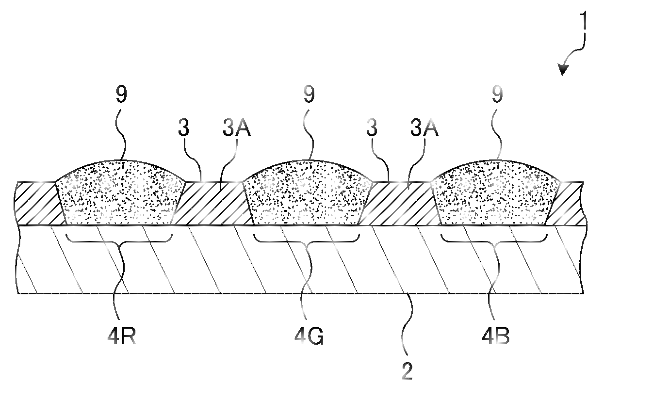
[0104]Hereinafter, manufacturing methods of organic EL display according to Embodiments 3 and 4 will be described with reference to the accompanying drawings. As illustrated in FIGS. 10A and 10B, the manufacturing methods according to Embodiments 3 and 4 eject ink droplets 11 on regions bank 3 adjacent to the widthwise ends of pixel region 4. The other aspects of the manufacturing methods according to Embodiments 3 and 4 are the same as those of the manufacturing method according to Embodiment 1. The same components as those of Embodiments 1 and 2 are given the same reference signs and the description of such components is not given in Embodiments 3 and 4.

[0105]More specifically, in Embodiment 3 where pixel regions 4R and 4G and 4B are grouped into sets of three, ink droplets 21 are landed on a lyophobic portion between each group of pixel regions 4 (FIG. 10A), the lyophobic portion being bank region 20 made of the same material as bank. On the other hand, in Embodiment 4, ink dropl...


PUM

PropertyMeasurementUnit
Contact angleaaaaaaaaaa

Abstract

A coating method in which ink droplets containing functional material are ejected through nozzles on a substrate having a plurality of pixel regions and lyophobic portions adjacent to the respective pixel regions, to form a functional layer in each of the pixel regions includes: landing an ink droplet on a first pixel region and on a first lyophobic portion adjacent to the first pixel region; measuring a deviation of a landing position of the ink droplet on the first lyophobic portion from a set ink landing position; and ejecting an ink droplet on a second pixel region of the substrate while correcting the timing of ink ejection through the nozzles based on the deviation.

Description

CROSS REFERENCE TO RELATED APPLICATION[0001]This application is entitled and claims the benefit of Japanese Patent Application No. 2010-126480 filed on Jun. 2, 2010, the disclosure of which including the specification, drawings and abstract is incorporated herein by reference in its entirety.TECHNICAL FIELD[0002]This disclosure relates to a method of forming organic films by coating techniques, and a manufacturing method of an organic electroluminescent display (hereinafter abbreviated as an “organic EL display”).BACKGROUND ART[0003]Organic EL displays can be broadly classified into two types according to the method by which their organic light-emitting films are formed. The first type of organic EL displays has organic light-emitting layers that are formed by vapor deposition, a technique used when low-molecular weight organic material is employed as raw material. The other type of organic EL displays has organic light-emitting layers that are formed by the coating method, a techni...

Claims


Application Information

Patent Timeline
IPC IPC(8): C23C16/52
CPCH01L27/3211H01L51/56H01L51/0005H10K59/35H10K71/135H10K71/00
Inventor SUZUKI, NAOKI
Owner PANASONIC INTELLECTUAL PROPERTY MANAGEMENT CO LTD
Why Eureka
Try Eureka