Antenna, semiconductor device, and method of manufacturing antenna

a semiconductor device and antenna technology, applied in the direction of burglar alarm mechanical actuation, burglar alarm by hand-held articles removal, etc., can solve the problem of difficulty in adjusting the resonant frequency f to a desired value, and achieve the reduction of the electrode area of the capacitor, the prevention of the suppression of response sensitivity and a response range, and the effect of reducing the distance between the electrodes of the capacitor

Inactive Publication Date: 2011-12-22
SEMICON ENERGY LAB CO LTD
View PDF4 Cites 16 Cited by
  • Summary
  • Abstract
  • Description
  • Claims
  • Application Information

AI Technical Summary

Benefits of technology

[0024]In an aspect of the present invention to be disclosed, the distance between the electrodes of the capacitor can be reduced by reducing the thickness of the dielectric body of the capacitor. By reducing the distance between the electrodes of the capacitor, the area of the electrode of the capacitor can be reduced. The reduction in the area of the electrode of the capacitor leads to the prevention of the suppression of response sensitivity and a response range of a semiconductor device.

Problems solved by technology

Therefore, it is difficult to adjust the resonant frequency f to a desired value by the number of windings of the coil NL.

Method used


Image

  • Antenna, semiconductor device, and method of manufacturing antenna
  • Antenna, semiconductor device, and method of manufacturing antenna
  • Antenna, semiconductor device, and method of manufacturing antenna

Examples


Embodiment Construction

[0032]Embodiment of the present invention disclosed in this specification will be hereinafter described with reference to the accompanying drawings. Note that the invention disclosed in this specification can be carried out in a variety of different modes, and it is easily understood by those skilled in the art that the modes and details of the invention disclosed in this specification can be changed in various ways without departing from the spirit and scope thereof. Therefore, the present invention is not construed as being limited to description of the Embodiment. Note that, in the drawings hereinafter shown, the same portions or portions having similar functions are denoted by the same reference numerals, and repeated description thereof will be omitted.

[0033]This Embodiment is explained with reference to FIGS. 1A and 1B, FIGS. 2A to 2C, FIGS. 3A to 3C, FIGS. 4A to 4C, FIGS. 5A to 5C, and FIG. 6.

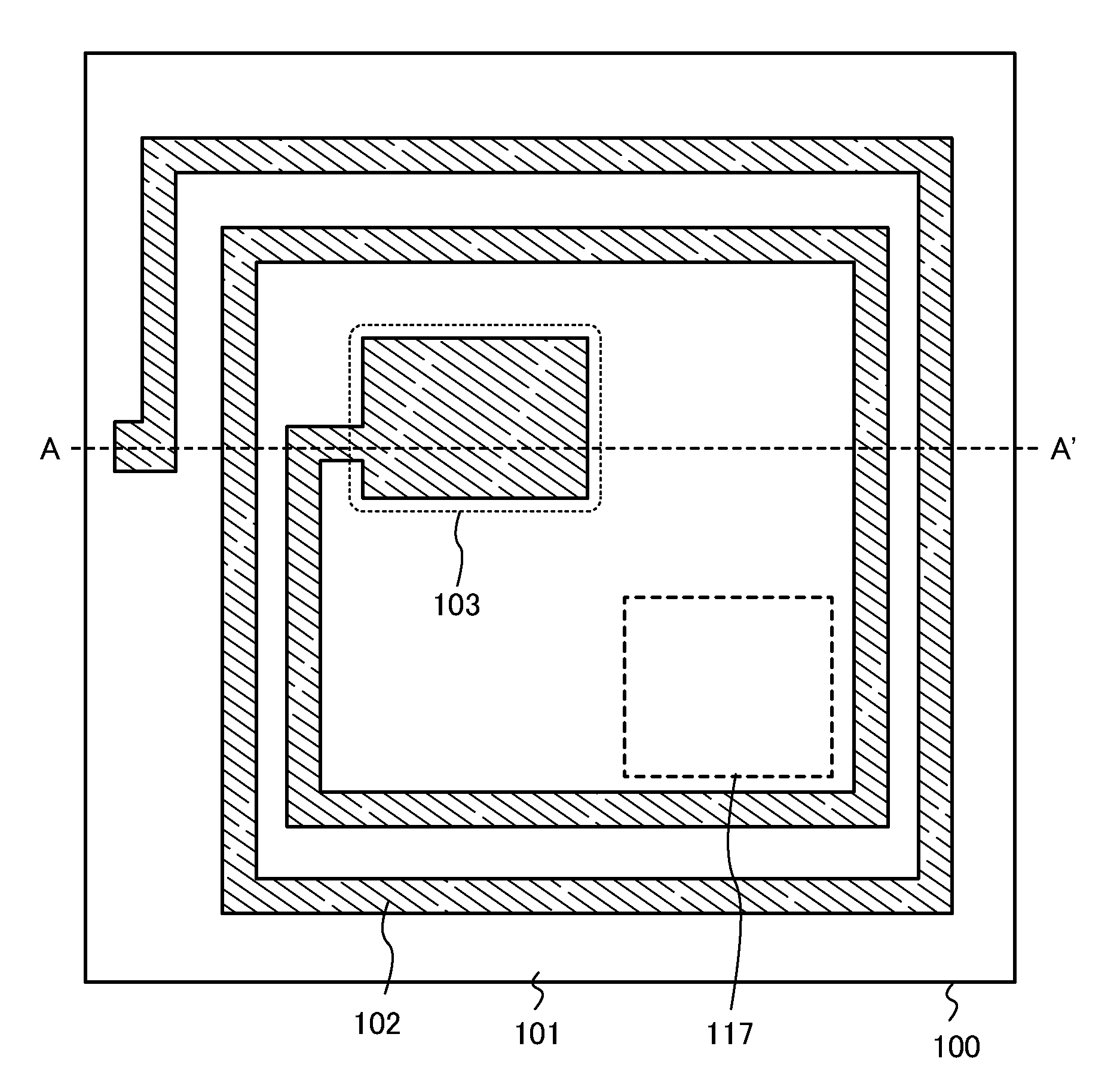
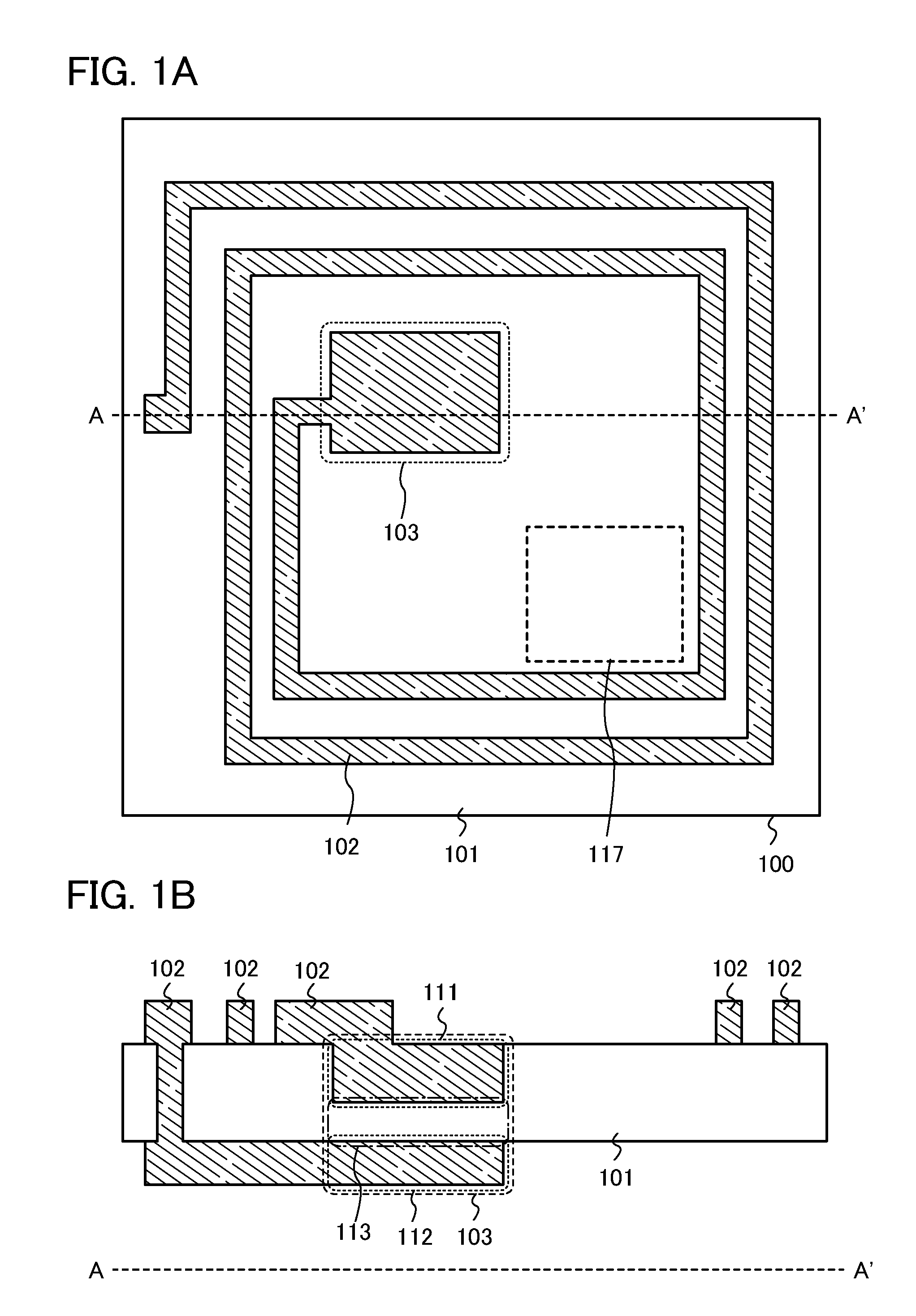
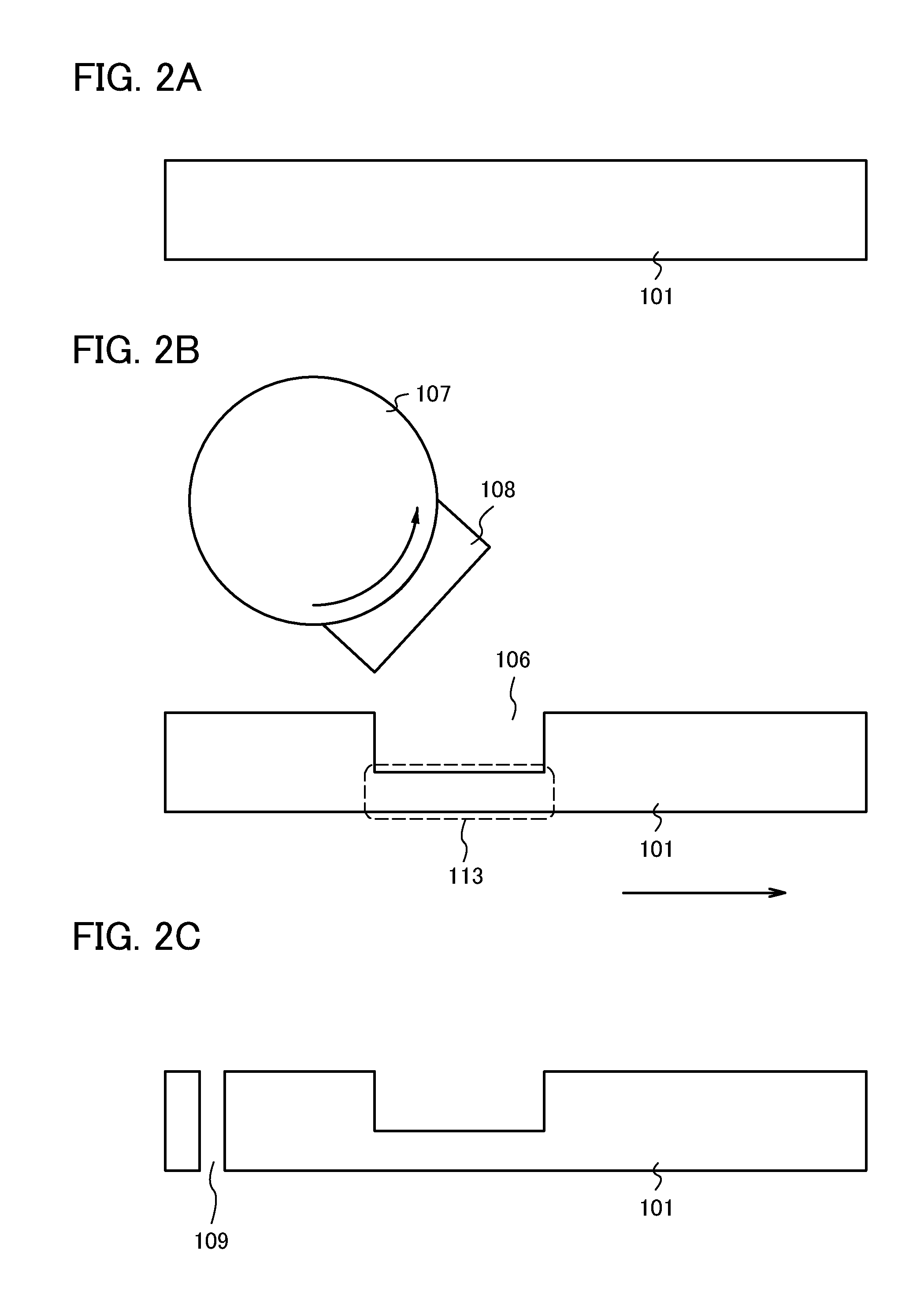
[0034]FIG. 1A is a top view of a semiconductor device 100, and FIG. 1B is a cross-se...


PUM

PropertyMeasurementUnit
thicknessaaaaaaaaaa
thicknessaaaaaaaaaa
thicknessaaaaaaaaaa

Abstract

In an antenna and a semiconductor device including the antenna, an object is to reduce the distance between electrodes of a capacitor as much as possible, reduce the area of the electrode of the capacitor as much as possible, and prevent the suppression of response sensitivity and a response range of the semiconductor device. The present invention relates to an antenna including an antenna coil provided over a first region of a base and a capacitor which uses a second region of the base as a dielectric body and which has electrodes provided for opposite planes of the second region of the base, wherein the second region of the base is thinner than the first region of the base, and also relates to a semiconductor device including the antenna.

Description

BACKGROUND OF THE INVENTION[0001]1. Field of the Invention[0002]An aspect of the present invention to be disclosed relates to a semiconductor device having a wireless communication function (also referred to as an ID tag).[0003]2. Description of the Related Art[0004]In recent years, an RFID system where data are exchanged between an ID tag (also referred to as an RFID tag, an IC tag, an electronic tag, or a wireless tag) and a reader / writer (or a reader) has been popular. Since data are exchanged using an antenna provided for each of an ID tag and a reader / writer in this RFID system, communication is possible even when the ID tag is set apart from the reader / writer by several centimeters to several meters. Moreover, due to an advantage of high resistance against dust, static electricity, and the like, the RFID system has come to be used for a variety of fields including production management in factories, logistics, access control, and the like.[0005]In a case of data communication ...

Claims


Application Information

Patent Timeline
Patent Type & Authority Applications(United States)
IPC IPC(8): H01F17/00H01P11/00
CPCG06K19/07773G06K19/07794H01F41/041Y10T29/49018H01Q7/00H01F5/003G06K19/077Y10T29/49016H01Q1/2225
Inventor AOKI, TOMOYUKISEKIGUCHI, SUSUMUEGUCHI, SHINGO
Owner SEMICON ENERGY LAB CO LTD
Why Eureka
Try Eureka