Touch panel and pixel aray thereof

a technology of pixel array and in-cell touch panel, which is applied in the field pixel array thereof, can solve problems such as degrading brightness performance, and achieve the effect of increasing the aperture ratio of in-cell touch panel

Inactive Publication Date: 2011-12-22
HANNSTAR DISPLAY CORPORATION
View PDF4 Cites 35 Cited by
  • Summary
  • Abstract
  • Description
  • Claims
  • Application Information

AI Technical Summary

Benefits of technology

[0009]The present invention provides a touch panel and pixel array thereof that may increase the aperture ratio of an in-cell touch panel.
[0010]The present invention further provides a touch panel with a dual gate line structure and pixel array thereof that may reduce the coupling effect between adjacent pixels thereby increasing the uniformity of the display.

Problems solved by technology

However, since the external touch panel will increase a total thickness of the touch screen and lower the transparency of the display device thereby degrading the brightness performance thereof, an in-cell touch panel is then proposed to solve this problem.

Method used


Image

  • Touch panel and pixel aray thereof
  • Touch panel and pixel aray thereof
  • Touch panel and pixel aray thereof

Examples


first embodiment

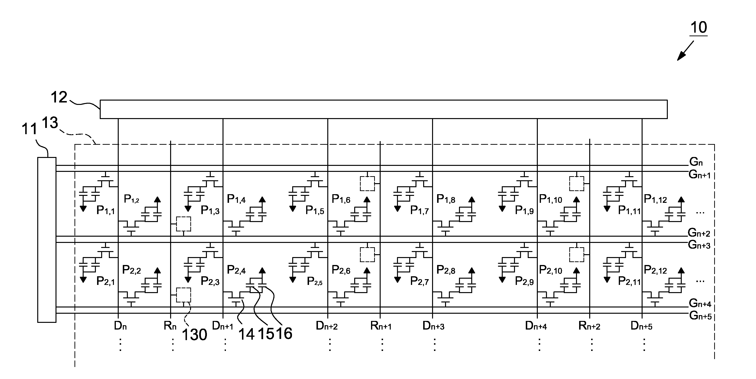
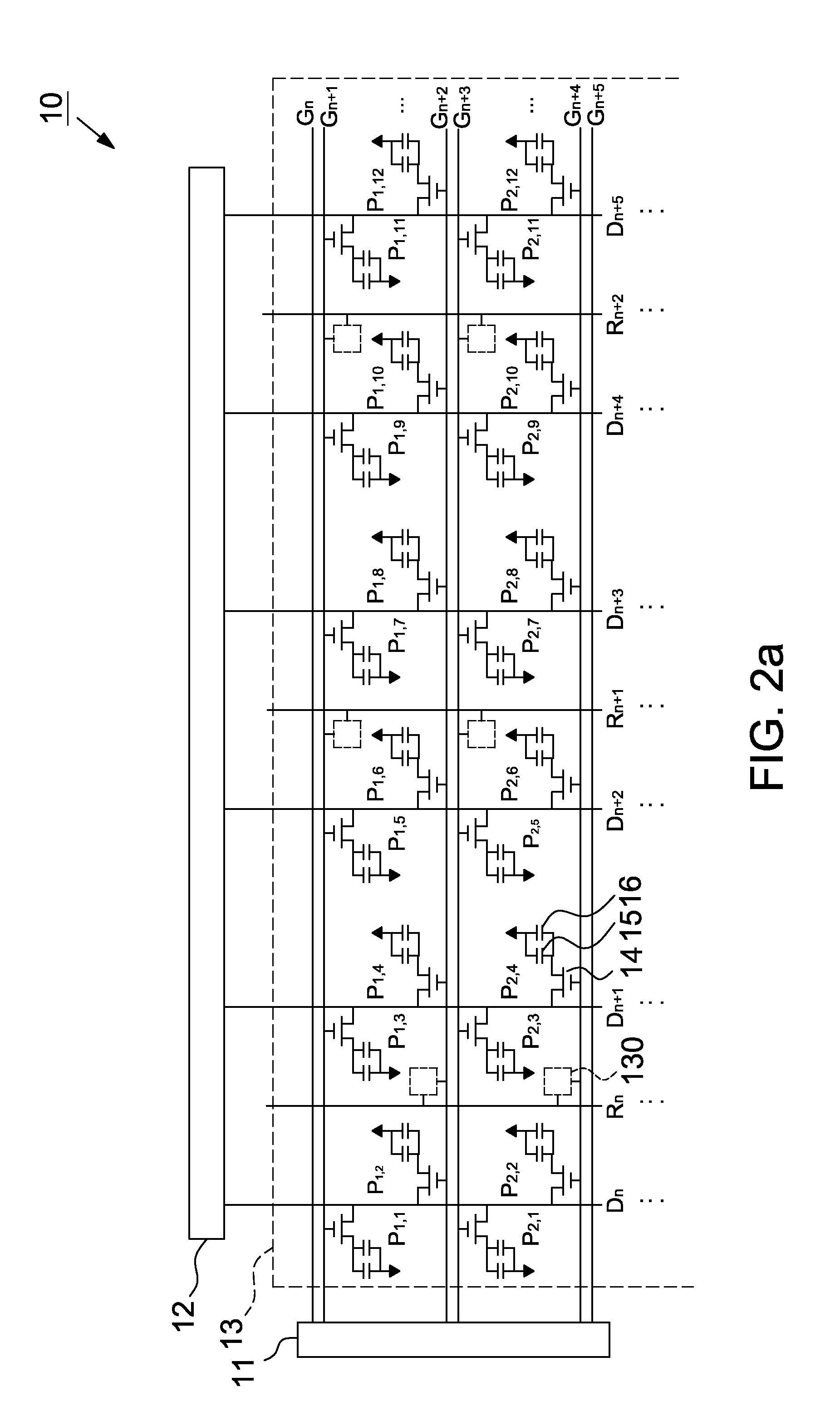
[0024]Please refer to FIGS. 2a and 2b, they show schematic diagrams of the touch panel 10 according to the present invention, wherein FIG. 2a shows a circuit schematic diagram of the touch panel 10 of this embodiment and FIG. 2b further shows the pixel structure of every pixel shown in FIG. 2a. As shown in FIG. 2a, the touch panel 10 includes a gate driver 11, a source driver 12 and a pixel array 13, which is an active matrix. The gate driver 11 sequentially outputs, in a scan period, a scan signal to every row of pixels of the pixel array 13 through a plurality of gate lines Gn˜G+5 extending in a horizontal direction and arranged in parallel. The source driver 12 outputs the gray level data to be displayed to every column of pixels of the pixel array 13 through a plurality of data lines Dn˜Dn+5 extending in a vertical direction and arranged in parallel, wherein the horizontal direction and the vertical direction are defined according to FIGS. 2a and 2b. It is appreciated that, the ...

second embodiment

[0035]In the second embodiment, as the readout lines are disposed between all adjacent pixels (or all adjacent pixel electrodes) having no data line disposed therebetween and a distance between adjacent data line and readout line is larger than a pixel electrode width W′ and less than a pixel width W or equal to a pixel width W, the coupling effect between adjacent pixels can be decreased thereby improving the uniformity of the display. In addition, since a data line and a readout line will not be disposed together between two adjacent pixels (or adjacent pixel electrodes), the present invention still has a higher aperture ratio than conventional in-cell touch panels.

[0036]Please refer to FIGS. 2 to 5, in a word the touch panel of the present invention includes a plurality of pixels arranged in a matrix, a plurality of gate lines, a gate driver coupled to the plurality of gate lines, a plurality of data lines and a plurality of readout lines. Every two pixels in a row along a horizo...


PUM


Abstract

A pixel array includes a plurality of pixels, data lines, readout lines and gate lines, wherein a data line and a readout line are alternatively disposed between every two adjacent pixels; two pixels adjacent to each data line are coupled to the same data line but coupled to different gate lines; and at least a part of the readout lines are coupled to one of the two pixels adjacent thereto. The present invention further provides a touch panel including the above pixel array.

Description

CROSS REFERENCE TO RELATED APPLICATION[0001]This application claims the priority benefit of Taiwan Patent Application Serial Number 099119829, filed on Jun. 18, 2010, the full disclosure of which is incorporated herein by reference.BACKGROUND[0002]1. Field of the Invention[0003]This invention generally relates to a touch control device and, more particularly, to an in-cell touch panel and pixel array thereof.[0004]2. Description of the Related Art[0005]The liquid crystal display is a widely used display device in the present day. With the maturity of the touch screen technologies, various kinds of electronic devices, e.g. a multimedia player, a cell phone and a personal digital assistance (PDA), generally are adopted with a LCD touch screen to increase the using convenience thereof.[0006]Conventional LCD touch screens include an external touch panel (or called touch sensor) attached in front of the LCD screen, so called add-on touch screen. Because resistive touch panels and capacit...

Claims


Application Information

Patent Timeline
Patent Type & Authority Applications(United States)
IPC IPC(8): G06F3/041
CPCG06F3/0412
Inventor JUAN, YI CHUNGLIN, SUNG CHUNYU, CHIA HUA
Owner HANNSTAR DISPLAY CORPORATION
Why Eureka
Try Eureka