Check patentability & draft patents in minutes with Patsnap Eureka AI!

Readout transistor circuits for CMOS imagers

Active Publication Date: 2011-12-29
SRI INTERNATIONAL
View PDF11 Cites 31 Cited by
  • Summary
  • Abstract
  • Description
  • Claims
  • Application Information

AI Technical Summary

Benefits of technology

[0012]The above-described problems are addressed and a technical solution achieved in the art by providing an improved readout circuit for a CMOS image sensor, comprising: a readout transistor circuit for a pixel, comprising: a sense node; a reset transistor in signal communication with the sense node; a source follower transistor in signal communication with the sense node; a row select transistor in signal communication with the source follower transistor; a switching transistor in signal communication with the sense node; and a capacitor in signal communication with the switching transistor, wherein the switching transistor is configured to place the capacitor in signal communication with the sense node to switch between a low voltage-per-charge (V / e−) ratio and a high voltage-per-charge (V / e−) to enable low noise performance of the sense node. The capacitor may be a metal-insulator-metal (MIM) capacitor. The metal-insulator-metal (MIM) capacitor may be connected in series with the switching transistor and the reset transistor, the MIM capacitor coupled between the switching transistor and the reset transistor. Alternatively, the switching transistor may be connected in parallel with the reset transistor.
[0016]The above-described problems are addressed and a technical solution achieved in the art by providing an imager, comprising: a pixel array comprising a plurality of pixels arranged in a predetermined number of columns and rows selected by a plurality of column select lines and row select lines, respectively; wherein each pixel of the pixel array comprises: a sense node; a reset transistor in signal communication with the sense node; a source follower transistor in signal communication with the sense node; a row select transistor in signal communication with the source follower transistor; a switching transistor in signal communication with the sense node; and a capacitor in signal communication with the switching transistor, wherein the switching transistor is configured to place the capacitor in signal communication with the sense node to switch between a low voltage-per-charge (V / e−) ratio and a high voltage-per-charge (V / e−) to enable low noise performance of the sense node. The capacitor may be metal-insulator-metal (MIM) capacitor.

Problems solved by technology

However, CCD imagers suffer from a number of disadvantages.
For example, CCDs are susceptible to radiation damage; CCDs are often expensive to manufacture; CCDs require good light shielding to avoid image smear and; CCDs have a high power dissipation for large arrays.
CCD imagers also have a complicated driving method and a complicated fabrication process requiring a multi-phased photo process.
A control circuit, a signal processing circuit, an analog to digital (A / D) converter circuit, etc., cannot be easily integrated into a CCD chip, thereby inhibiting the use of CCDs in compact size products.
While there have been some attempts to integrate on-chip signal processing with a CCD array, these attempts have not been entirely successful.
CCDs may also suffer from incomplete charge transfer from pixel to pixel during charge transfer which also results in image smear.
The second ADC has low front end gain and provides for an input signal of up to 25,000 e / pixel at saturation but has relatively high noise because of low front end gain.
This results in higher packaging costs, greater camera complexity and higher on-chip power dissipation.
Increased chip power dissipation is undesirable because it may result in a higher dark current, resulting in an imager that has reduced sensitivity or a need for increased cooling.

Method used


Image

  • Readout transistor circuits for CMOS imagers
  • Readout transistor circuits for CMOS imagers
  • Readout transistor circuits for CMOS imagers

Examples


Embodiment Construction

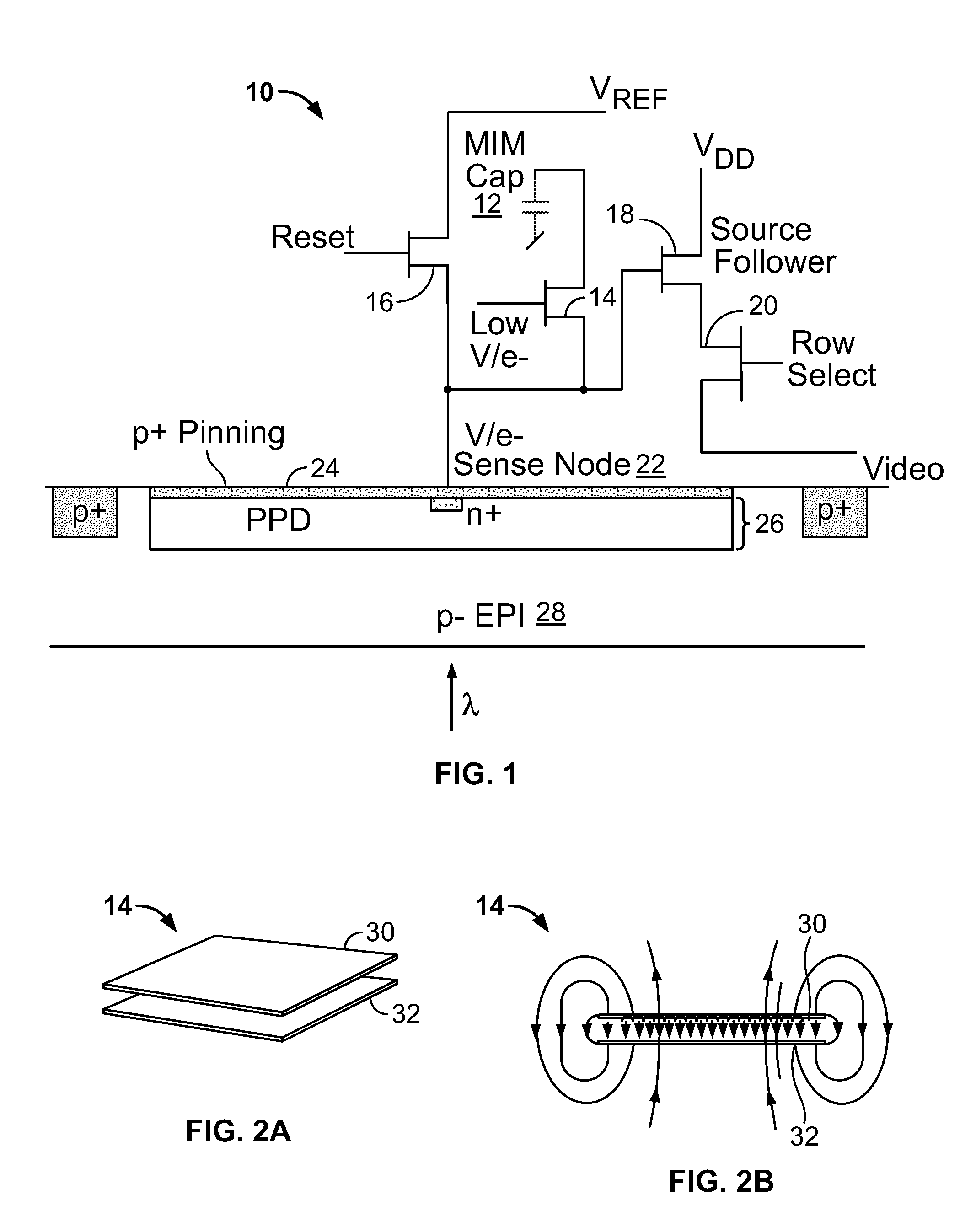
[0059]FIG. 1 depicts a side view of a high dynamic range back-illuminated n-type CMOS 4T pixel 10 (hereinafter an “n—4TPPD pixel 10”), according to an embodiment of the present invention. The n—4TPPD pixel 10 is formed from a conventional n-type CMOS 3T pixel having three NMOS type readout transistors with the addition of a metal-insulator-metal (MIM) capacitor 12 and a MOSFET 14 (hereinafter “the MIM MOSFET 14”). The n—4TPPD pixel 12 includes a reset transistor 16, a source follower transistor 18, and a row select transistor 20 communicatively connected to a sense node 22. The sense node 22 comprises a thin p+ layer 24 for pinning a pixel photodiode (PPD) 26. The PPD 26 is formed in a p− epi layer 28. As illustrated in FIG. 1, a high dynamic range n—4TPPD pixel 10 results when the MIM capacitor 12 is switched onto the sense node 22 with the MIM MOSFET 14. One terminal of the MIM capacitor 12 is electrically connected to the source terminal of the MIM MOSFET 14. A second terminal of...


PUM


Abstract

A readout transistor circuit for a pixel is disclosed. The readout transistor circuit includes a sense node. A reset transistor is in signal communication with the sense node. A source follower transistor is in signal communication with the sense node. A row select transistor is in signal communication with the source follower transistor. A switching transistor is in signal communication with the sense node. A capacitor is in signal communication with the switching transistor. The switching transistor is configured to place the capacitor in signal communication with the sense node to switch between a low voltage-per-charge (V / e−) ratio and a high voltage-per-charge (V / e−) to enable low noise performance of the sense node. The capacitor may be a metal-insulator-metal (MIM) capacitor. At least one of the reset transistor, the source follower transistor, the row select transistor, and the switching transistor may be a MOSFET. One or more of the MOSFETs may be a buried channel MOSFET.

Description

CROSS-REFERENCES TO RELATED APPLICATIONS[0001]This application claims the benefit of U.S. provisional patent application No. 61 / 358,921 filed Jun. 27, 2010, and U.S. provisional patent application No. 61 / 407,993 filed Oct. 29, 2010, the disclosures of which are incorporated herein by reference in their entirety. This application is also related to copending U.S. Utility patent application Ser. No. 12 / 844,054, filed Jul. 27, 2010, the disclosure of which is incorporated by reference in its entirety.FIELD OF THE INVENTION[0002]The invention relates generally to imaging devices. More specifically, the invention relates to improving the performance of transistor readout circuits employed in CMOS imagers.BACKGROUND OF THE INVENTION[0003]Generally, an image sensor is a semiconductor device for converting an optical image into an electric signal. There are a number of different types of semiconductor-based imagers, including charge coupled devices (CCDs), photodiode arrays, charge injectio...

Claims


Application Information

Patent Timeline
IPC IPC(8): H01L27/146G01J1/46
CPCG01J1/46H01L27/1203H01L27/14614H04N5/37452H01L27/14643H01L28/40H04N5/3559H01L27/1464H04N25/59H04N25/771
Inventor JANESICK, JAMES ROBERT
Owner SRI INTERNATIONAL
Features
  • R&D
  • Intellectual Property
  • Life Sciences
  • Materials
  • Tech Scout
  • Unparalleled Data Quality
  • Higher Quality Content
  • 60% Fewer Hallucinations
Learn More