
Power semiconductor device

a technology of semiconductor devices and semiconductors, applied in the direction of semiconductor devices, electrical equipment, transistors, etc., can solve the problems of increasing device size, generating large amount of heat from conduction loss, and reducing the life of power cycles, so as to prevent a temperature rise in the central portion of the substra

Active Publication Date: 2011-12-29
SONRAI MEMORY LTD
View PDF6 Cites 12 Cited by
  • Summary
  • Abstract
  • Description
  • Claims
  • Application Information

AI Technical Summary

Benefits of technology

"The present invention provides a power semiconductor device that prevents temperature rise in the central portion of a substrate that affects the entire substrate. This is achieved by a resistance control structure that makes the resistance higher in the central portion of the substrate compared to the peripheral portion. This reduces heat generation and prevents temperature rise in the central portion, improving the reliability of the power cycle life and avoiding the need for a temperature detecting element that increases device size."

Problems solved by technology

Power semiconductor devices such as an insulated gate bipolar transistor (IGBT) handle a large amount of power, and as a result generate large amount of heats from conduction loss.
Large temperature rise, temperature change or the like incurs, for example, fatigue of a wire-bonded portion, thus leading to a reduction in power cycle life.
However, in the semiconductor device of Japanese Patent Application Laid-Open No. 06-342876, the region in which the temperature detecting element is disposed needs to be secured, which leads to an increase in device size.

Method used


Image

  • Power semiconductor device
  • Power semiconductor device
  • Power semiconductor device

Examples


first preferred embodiment

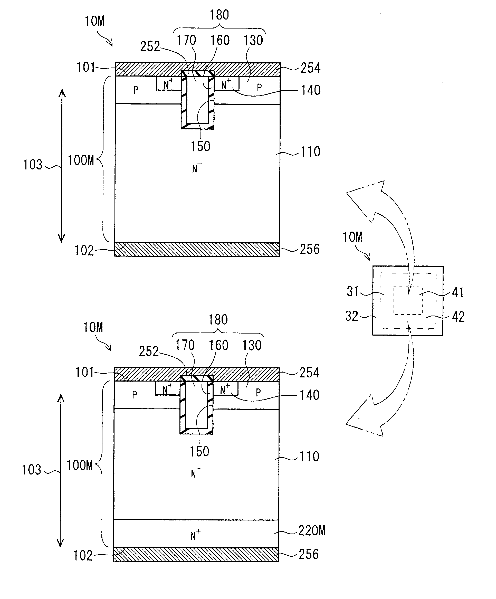
[0044]In a first preferred embodiment, an IGBT is described as an example of a power semiconductor device. FIG. 1 is a plan view (in other words, top view) of a semiconductor chip of an IGBT 10A according to the first preferred embodiment. The IGBT 10A includes at least the semiconductor chip, and may include a bonding wire connected to the semiconductor chip and an insulating substrate on which the semiconductor chip is mounted, or the like. While the following description will be given of one semiconductor chip included in the IGBT 10A, the IGBT 10A may include a plurality of semiconductor chips.

[0045]In an example of FIG. 1, the semiconductor chip of the IGBT 10A can be roughly divided into an element portion 31 and a terminal portion 32. The element portion 31 is a region in which a plurality of power semiconductor elements (in this case, a plurality of IGBT unit elements) are disposed, for example, in matrix. The terminal portion 32 is a region in which a structure (for example...

second preferred embodiment

[0087]FIG. 5 schematically shows an IGBT 10B according to a second preferred embodiment. For simplification of the description, the right part of FIG. 5 shows a plan view corresponding to FIG. 1, the upper-left part thereof shows a vertical cross-sectional view of the central portion 41, and the lower-left part thereof shows a vertical cross-sectional view of the peripheral portion 42.

[0088]The IGBT 10B fundamentally has a similar configuration to that of the IGBT 10A (see FIG. 1 and FIG. 2) except for that the IGBT 10B includes a semiconductor substrate 100B in place of the semiconductor substrate 100A (see FIG. 2). The semiconductor substrate 100B fundamentally has a similar configuration to that of the semiconductor substrate 100A except for that the semiconductor substrate 100B includes a collector layer 200B in place of the collector layer 200A (see FIG. 2).

[0089]FIG. 6 is a perspective view schematically showing the collector layer 200B. FIG. 6 shows the collector layer 200B e...

third preferred embodiment

[0094]FIG. 7 is a vertical cross-sectional view schematically showing an IGBT 10C according to a third preferred embodiment. The IGBT 10C fundamentally has a similar configuration to that of the IGBT 10A (see FIG. 1 and FIG. 2) except for that the IGBT 10C includes a semiconductor substrate 100C in place of the semiconductor substrate 100A (see FIG. 2). The semiconductor substrate 100C fundamentally has a similar configuration to that of the semiconductor substrate 100A except for that the semiconductor substrate 100C includes a collector layer 200 in place of the collector layer 200A (see FIG. 2) and that a lifetime control layer 210C is added.

[0095]The collector layer 200 has the same impurity concentration between the central portion 41 and the peripheral portion 42, and other conditions are configured similarly to the collector layer 200A (see FIG. 2).

[0096]The lifetime control layer 210C is provided in the drift layer 110 and extends with the substrate thickness direction 103 a...


PUM


Abstract

Provided is a power semiconductor device including a semiconductor substrate, in which a current flows in a thickness direction of the semiconductor substrate. The semiconductor substrate includes a resistance control structure configured so that a resistance to the current becomes higher in a central portion of the semiconductor substrate than a peripheral portion of the semiconductor substrate.

Description

BACKGROUND OF THE INVENTION[0001]1. Field of the Invention[0002]The present invention relates to a power semiconductor device.[0003]2. Description of the Background Art[0004]Power semiconductor devices such as an insulated gate bipolar transistor (IGBT) handle a large amount of power, and as a result generate large amount of heats from conduction loss. Accordingly, the temperature of a semiconductor substrate increases greatly, and the temperature varies largely by an on / off operation.[0005]Large temperature rise, temperature change or the like incurs, for example, fatigue of a wire-bonded portion, thus leading to a reduction in power cycle life. Note that the power cycle life is one indication of the reliability of a power semiconductor device, which indicates the life influenced by, for example, peeling of a wire bonding portion due to a temperature change incident to an operation.[0006]It is considered that, in a power semiconductor device, temperature becomes higher in a central...

Claims


Application Information

Patent Timeline
Patent Type & Authority Applications(United States)
IPC IPC(8): H01L29/78H01L29/868
CPCH01L29/0696H01L29/0834H01L29/7395H01L29/7397H01L29/36H01L29/66333H01L29/66348
Inventor HATORI, KENJI
Owner SONRAI MEMORY LTD
Learn More