LED chip testing device

a chip testing and led chip technology, applied in the direction of measurement devices, electrical testing, instruments, etc., can solve the problems of inability to obtain accurate analysis, inability to find inferior goods or lower classes of led chips, time-consuming and cost-ineffective, etc., to achieve accurate testing of led chips

Inactive Publication Date: 2011-12-29
QMC
View PDF41 Cites 27 Cited by
  • Summary
  • Abstract
  • Description
  • Claims
  • Application Information

AI Technical Summary

Benefits of technology

[0018]In accordance with an embodiment of the present invention, the size of the passing hole may be gradually reduced in a direction facing toward the LED chip located at the testing position from the measurement unit.

Problems solved by technology

That is, even in case no problem that affects the performance of LEDs is generated in the packaging process, the LEDs can be found to be inferior goods or sorted into lower classes due to the problems that are generated while the LED chips are fabricated.
The LEDs that are excluded as the inferior goods in the testing process due to the problems caused when the LED chips are fabricated are undergone through the packaging process and the testing process unnecessarily.
As they undergo through the unnecessary processes, loss in material costs and process costs may be caused.
As a result, it has been time-consuming and cost ineffective in obtaining accurate analysis results.
The above-mentioned problems may result in an increase of a unit cost for the manufacture of products using LEDs as well as an increase of a unit cost for the manufacture of LEDs.

Method used


Image

  • LED chip testing device
  • LED chip testing device
  • LED chip testing device

Examples


Embodiment Construction

[0049]Hereinafter, embodiments of an LED chip testing device in accordance with the present invention will be described in detail with reference to the accompanying drawings.

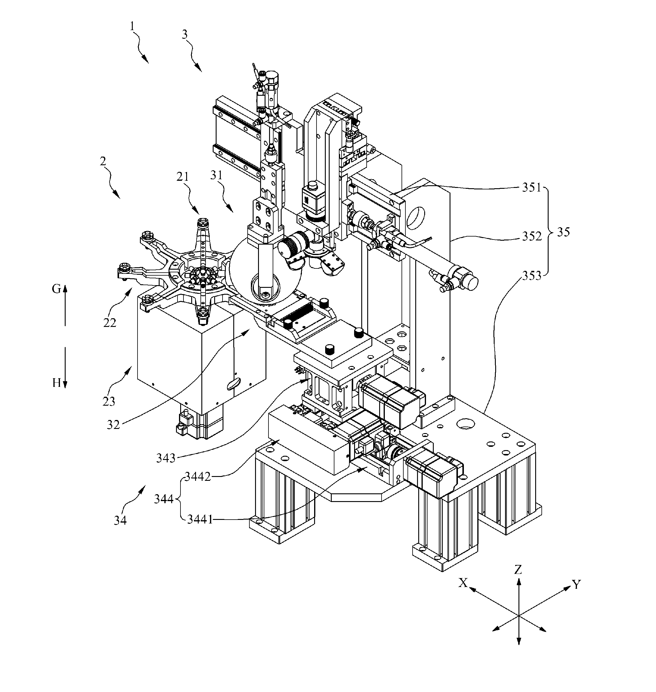
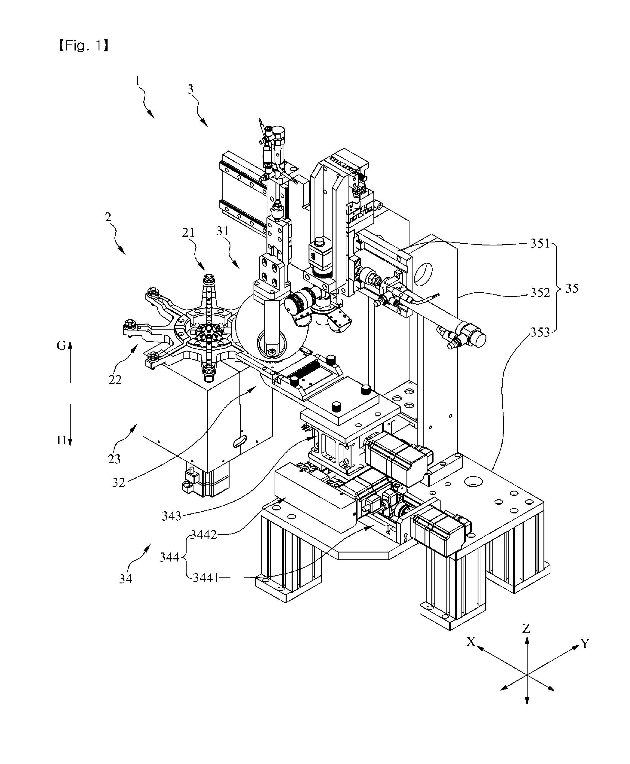
[0050]Referring to FIG. 1, the LED chip testing device 1 includes the feeder 2 and the tester 3. The tester 3 includes the measurement unit 31, the contact unit 32, the first conveyance member 33 (shown in FIG. 8), the contact movement member 34 and the main body 35.

Feeder

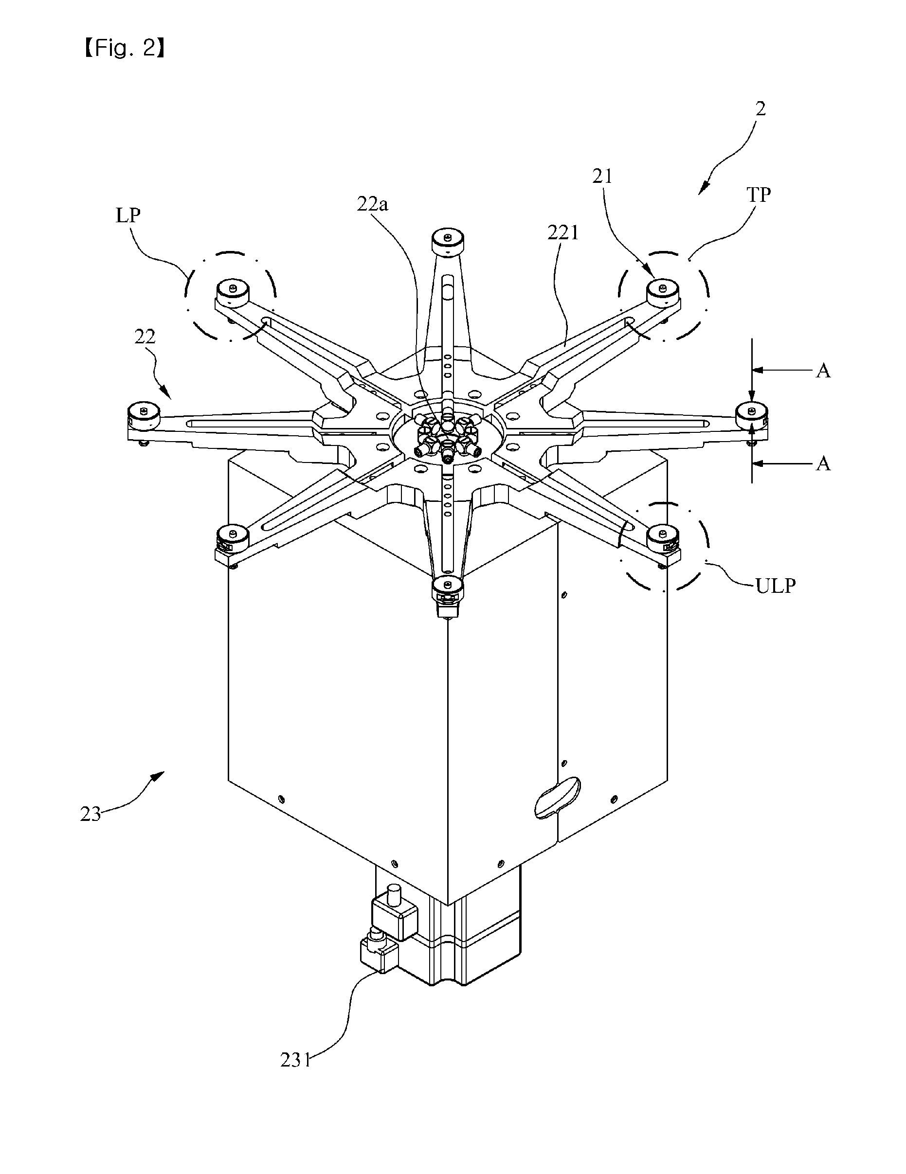
[0051]Referring to FIGS. 1 and 2, the feeder feeds a to-be-tested LED chip to a testing position where the measurement unit 31 is capable of measuring an optical characteristic of the LED chip. The feeder 2 may include one or more mounting members 21, a rotation member 22 and a rotation unit 23.

[0052]Referring to FIGS. 1 to 3, an LED chip is mounted on the mounting member 21. After the LED chip is mounted on the mounting table, the LED chip is attracted onto the mounting member 21 to be firmly held thereon by an air suctioning device F (shown ...


PUM


Abstract

The present invention provides an LED chip testing device that measures characteristics of an LED chip.The LED chip testing device includes: a rotation member that supports the LED chip and rotates the LED chip to a testing position where the characteristics of the LED chip are tested; and a tester installed next to the rotation member and serving to measure the characteristics of the LED chip at the testing position.

Description

FIELD OF THE INVENTION [0001]The present invention relates to an LED chip testing device that tests LED chips to investigate their performance.BACKGROUND OF THE INVENTION [0002]A light emitting diode (LED) is a kind of semiconductor light emitting device that converts electricity to light. The LED is also called a luminescent diode. The LED presents many advantages over conventional light sources, including smaller size, longer lifetime, low power consumption and high-speed responsiveness. Thus, the LED has been widely utilized in various applications such as a display device for an automotive instrument, a display lamp for various electronic devices such as an optical communication light source, a card reader for a numeric display device or a calculator, a backlight, and so forth.[0003]The LED is manufactured through an EPI process, a chip process (fabrication) and a packaging process. The LED is subjected to a testing process after it is packaged through the packaging process. In ...

Claims


Application Information

Patent Timeline
Patent Type & Authority Applications(United States)
IPC IPC(8): G01R31/26
CPCG01R31/2635G01R31/2893G01R31/2887
Inventor RYU, BENG SO
Owner QMC
Why Eureka
Try Eureka