
Avoiding degradation of chalcogenide material during definition of multilayer stack structure

a technology of chalcogenide and multilayer stack structure, applied in the direction of electrical equipment, nanotechnology, semiconductor devices, etc., can solve the problems of non-volatility and soft error rate, high programming voltage, endurance and reliability problems

Active Publication Date: 2012-01-05
MICRON TECH INC
View PDF5 Cites 76 Cited by
  • Summary
  • Abstract
  • Description
  • Claims
  • Application Information

AI Technical Summary

Problems solved by technology

Embedded SRAM (Static Random Access Memory) and DRAM (Dynamic Random Access Memory) have problems with non-volatility and soft error rates, while embedded flash memories require additional masking layers / processing steps during manufacture, require high-voltage for programming, and have issues with endurance and reliability.

Method used


Image

  • Avoiding degradation of chalcogenide material during definition of multilayer stack structure
  • Avoiding degradation of chalcogenide material during definition of multilayer stack structure
  • Avoiding degradation of chalcogenide material during definition of multilayer stack structure

Examples


Embodiment Construction

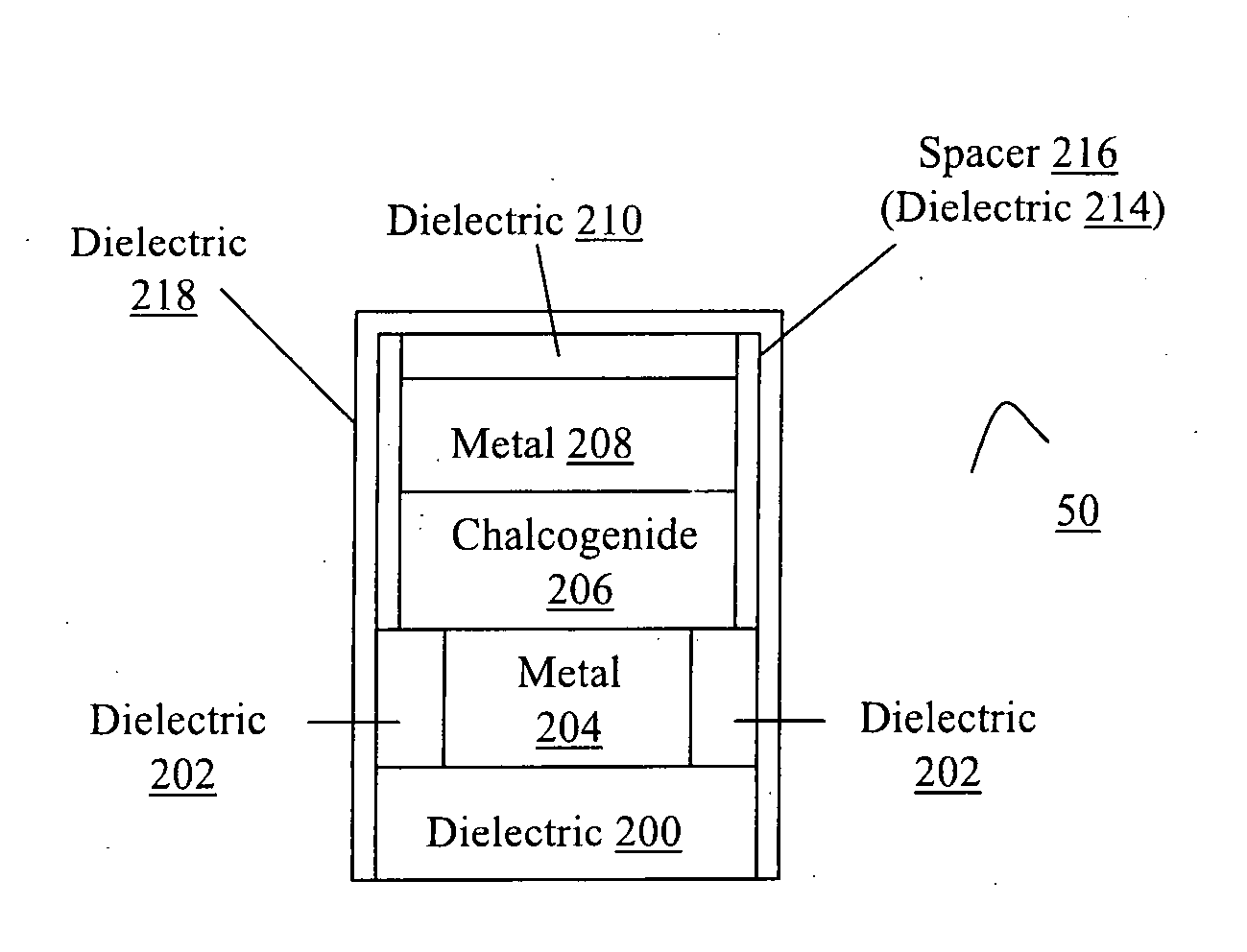
[0018]In the following detailed description, an integration scheme is disclosed for the fabrication of PCM cells in microelectronic devices. Reference is made to the accompanying drawings within which are shown, by way of illustration, specific embodiments by which the present invention may be practiced. It is to be understood that other embodiments may exist and that other changes may be made without departing from the scope and spirit of the present invention.

[0019]In addition, specific details such as specific materials are set forth herein in order to provide a thorough understanding of the present invention. However, it will be apparent to one skilled in the art that the present invention may be practiced without these specific details. In other instances, well known processing steps and / or microelectronic device elements have not been described in detail in order not to unnecessarily obscure the present invention. For example, well-known cleaning steps, protective layers, and / ...


PUM


Abstract

A storage element structure for phase change memory (PCM) cell and a method for forming such a structure are disclosed. The method of forming a storage element structure, comprises providing a multilayer stack comprising a chalcogenide layer (206), a metal cap layer (208), and a dielectric hard mask layer (210), depositing and patterning a photo resist layer (212) on top of the multilayer stack, etching the dielectric hard mask layer using the photo resist layer as etch mask, after the dielectric hard mask layer is etched, removing the photo resist layer before etching the chalcogenide, etching the chalcogenide layer using the dielectric hard mask layer as etch mask, depositing a spacer dielectric (214) over the multilayer stack and anisotropically etching the spacer dielectric to form sidewall spacers (216) for the multilayer stack.

Description

BACKGROUND OF THE INVENTION[0001]1. Field of the Invention[0002]The present invention relates to Phase Change Memory (PCM) cells and a fabrication method thereof.[0003]2. Description of the Related Art[0004]Embedded SRAM (Static Random Access Memory) and DRAM (Dynamic Random Access Memory) have problems with non-volatility and soft error rates, while embedded flash memories require additional masking layers / processing steps during manufacture, require high-voltage for programming, and have issues with endurance and reliability. PCM overcomes the criticality of the above mentioned parameters and exhibits favorable write speeds, small cell sizes, simpler circuitries and a fabrication compatibility with the Complementary Metal-Oxide-Semiconductor (CMOS) process. However, additional improvements are needed in the evolution of the PCM technology.BRIEF DESCRIPTION OF THE DRAWINGS[0005]The subject matter regarded as the invention is particularly pointed out and distinctly claimed in the co...

Claims


Application Information

Patent Timeline
IPC IPC(8): H01L21/20H01L45/00B82Y40/00B82Y99/00
CPCH01L27/2445H01L45/06H01L45/1675H01L45/126H01L45/144H01L45/1233H10B63/32H10N70/8413H10N70/231H10N70/8828H10N70/063H10N70/826
Inventor MAGISTRETTI, MICHELEPETRUZZA, PIETROSCIARRILLO, SAMUELECASELLATO, CRISTINA
Owner MICRON TECH INC
Features
  • Generate Ideas
  • Intellectual Property
  • Life Sciences
  • Materials
  • Tech Scout
  • Unparalleled Data Quality
  • Higher Quality Content
  • 60% Fewer Hallucinations
Learn More