Light emitting device module
a technology of light-emitting devices and modules, which is applied in the direction of semiconductor devices for light sources, lighting and heating apparatus, and light-emitting support devices, etc., can solve the problems of additional costs, and achieve the effects of convenient coupling, easy notice, and easy slide on the printed circuit board
- Summary
- Abstract
- Description
- Claims
- Application Information
AI Technical Summary
Benefits of technology
Problems solved by technology
Method used
Image

Examples
Embodiment Construction
[0002]1. Technical Field
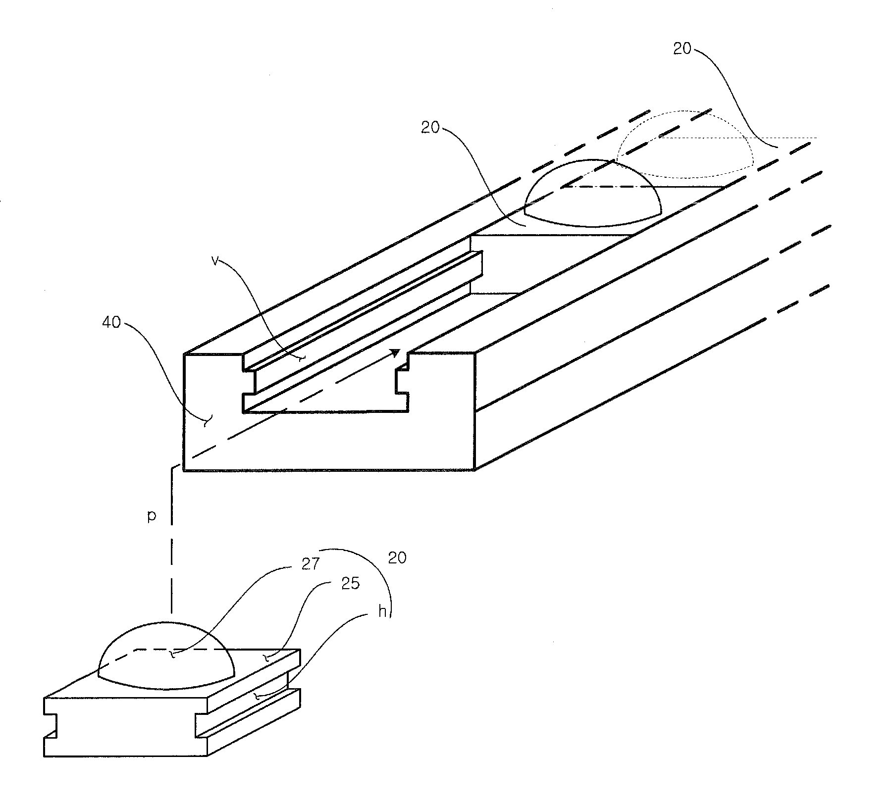
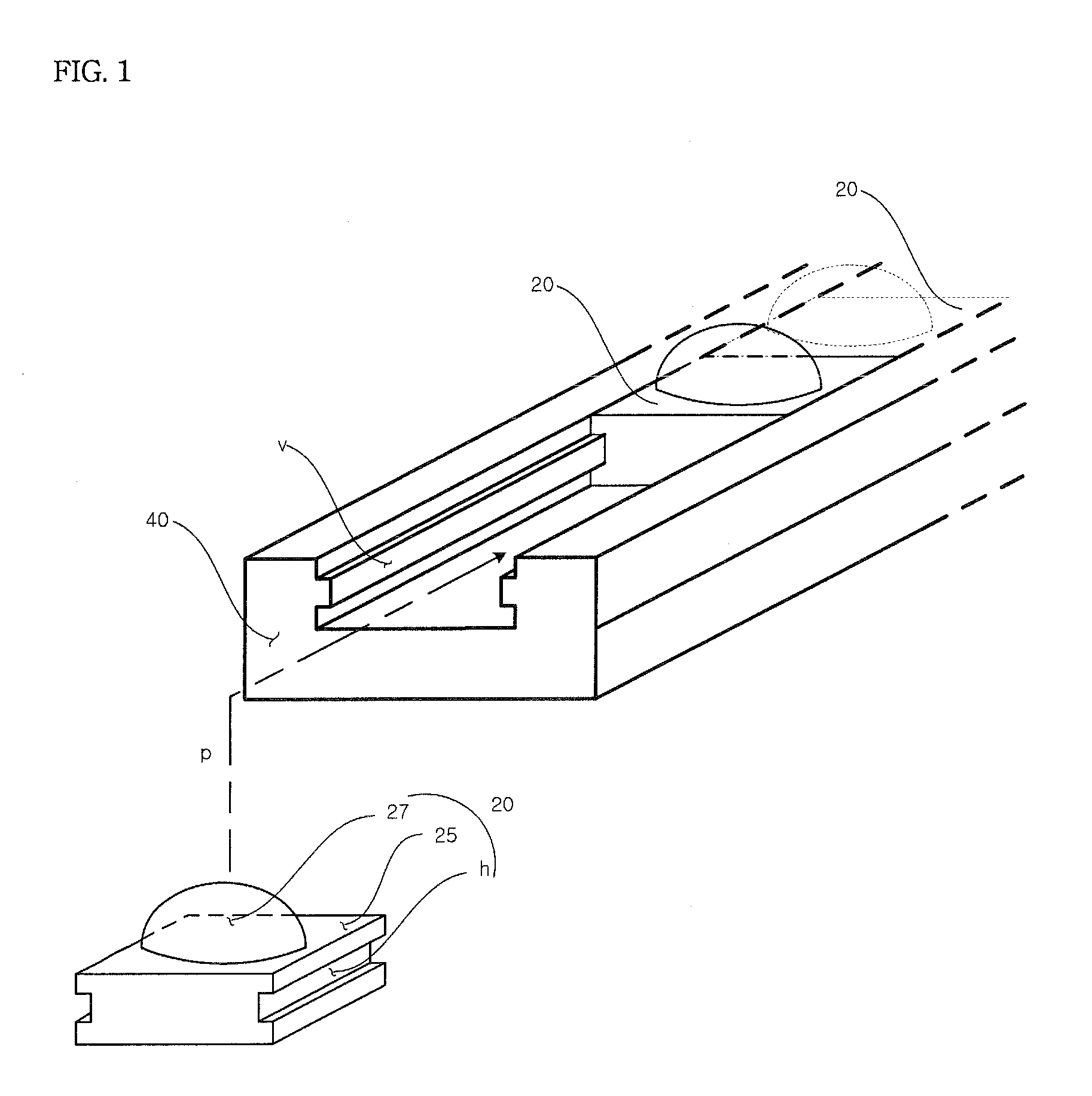
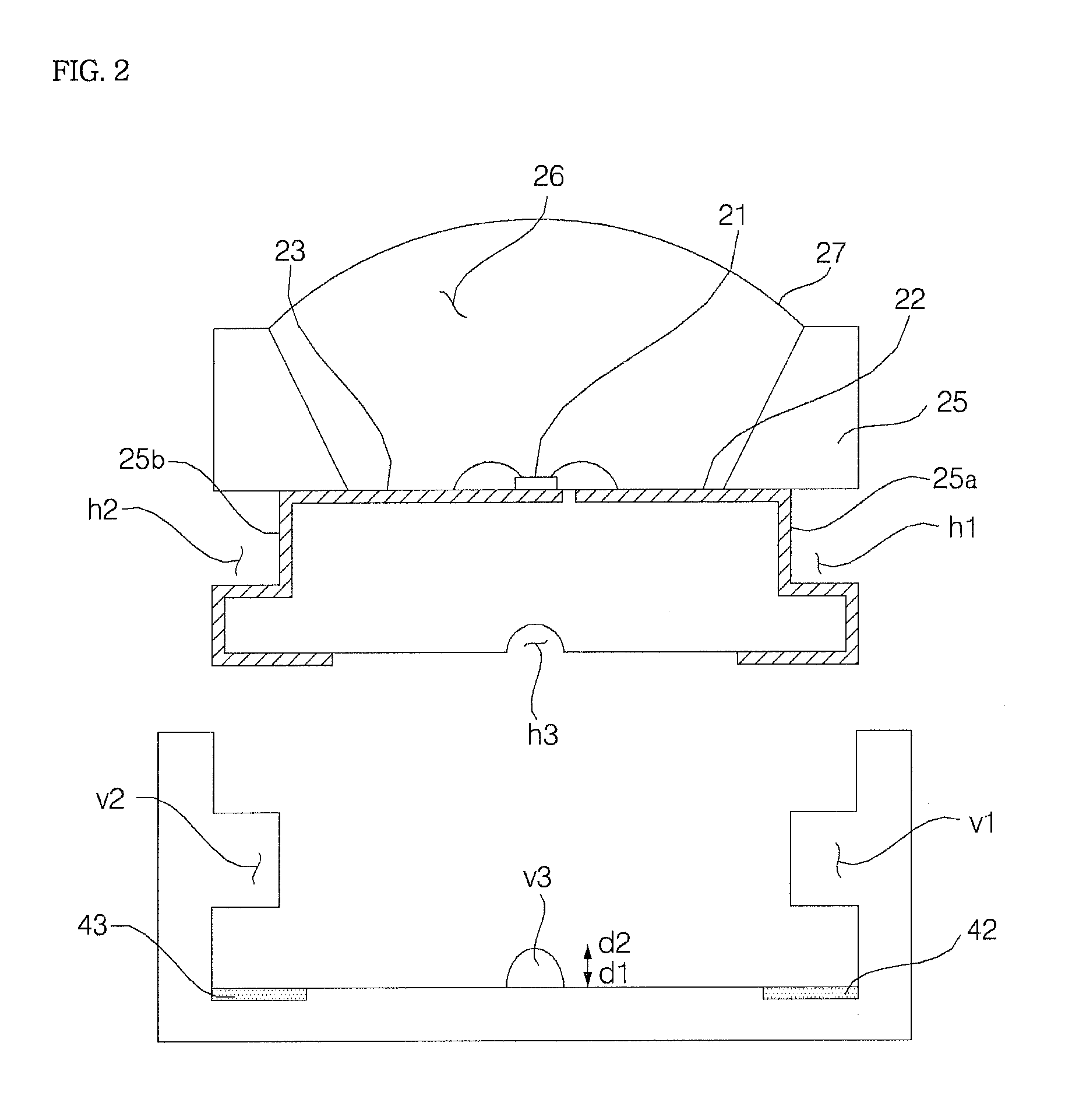
[0003]Exemplary embodiments are directed to a light emitting device module, and more specifically to a light emitting device module that includes a light emitting device package and a printed circuit board, wherein the light emitting device package is easily detachable from the printed circuit board.
[0004]2. Discussion of the Related Art
[0005]In general, a light emitting diode (LED) includes a light emitting device, lead pins for power feeding, and a sealing material for protecting the light emitting device. A diversity of light emitting devices may emit infrared beams, ultraviolet rays, or visible rays. Light emitting device packages have various applications, such as sensors, displays, or illumination.
[0006]The lead pins of the light emitting device package are connected to electrodes formed on a printed circuit board or a power cable to supply power to the light emitting device package.
[0007]The lead pins of the light emitting device package include + / − le...
PUM
 Abstract
Description
Claims
Application Information
 - R&D
- Intellectual Property
- Life Sciences
- Materials
- Tech Scout
- Unparalleled Data Quality
- Higher Quality Content
- 60% Fewer Hallucinations
Browse by: Latest US Patents, China's latest patents, Technical Efficacy Thesaurus, Application Domain, Technology Topic, Popular Technical Reports.
© 2025 PatSnap. All rights reserved.Legal|Privacy policy|Modern Slavery Act Transparency Statement|Sitemap|About US| Contact US: help@patsnap.com