Substrate cleaning method and substrate cleaning device

a cleaning method and substrate technology, applied in the direction of cleaning process and apparatus, cleaning using liquids, chemistry apparatus and processes, etc., can solve the problems of fine droplets adhering to the hydrophobic portion, substrate processing defects, etc., and achieve the effect of preventing substrate processing defects

Active Publication Date: 2012-01-12
SCREEN SEMICON SOLUTIONS CO LTD
View PDF5 Cites 39 Cited by
  • Summary
  • Abstract
  • Description
  • Claims
  • Application Information

AI Technical Summary

Benefits of technology

[0010]An object of the present invention is to provide a substrate cleaning method and a substrate cleaning device capable of preventing processing defects of a substrate from being caused by a rinse liquid adhering to the substrate.

Problems solved by technology

It is difficult to shake off fine droplets adhering to the hydrophobic portion by a centrifugal force.
As a result, when the substrate is unevenly dried with remaining fine droplets after the spin drying, reaction products such as water marks are produced, leading to processing defects of the substrate.

Method used


Image

  • Substrate cleaning method and substrate cleaning device
  • Substrate cleaning method and substrate cleaning device
  • Substrate cleaning method and substrate cleaning device

Examples


Embodiment Construction

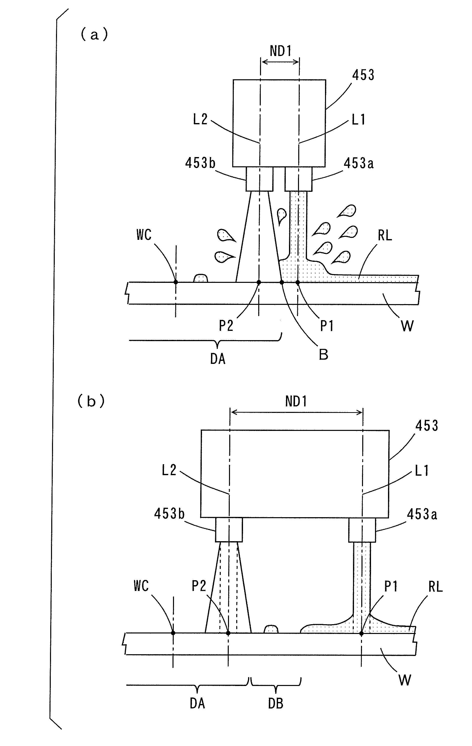
[0069]Description will be made of a substrate cleaning method and a substrate cleaning device according to one embodiment of the present invention while referring to the drawings. In the following description, a substrate refers to a semiconductor substrate, a substrate for a liquid crystal display, a substrate for a plasma display, a glass substrate for a photomask, a substrate for an optical disk, a substrate for a magnetic disk, a substrate for a magneto-optical disk, a substrate for a photomask or the like.

[0070]The substrate cleaning method according to the one embodiment of the present invention is used in a substrate processing apparatus described below. In the following paragraphs, description will be made of a development processing device provided in the substrate processing apparatus as one example of the substrate cleaning device.

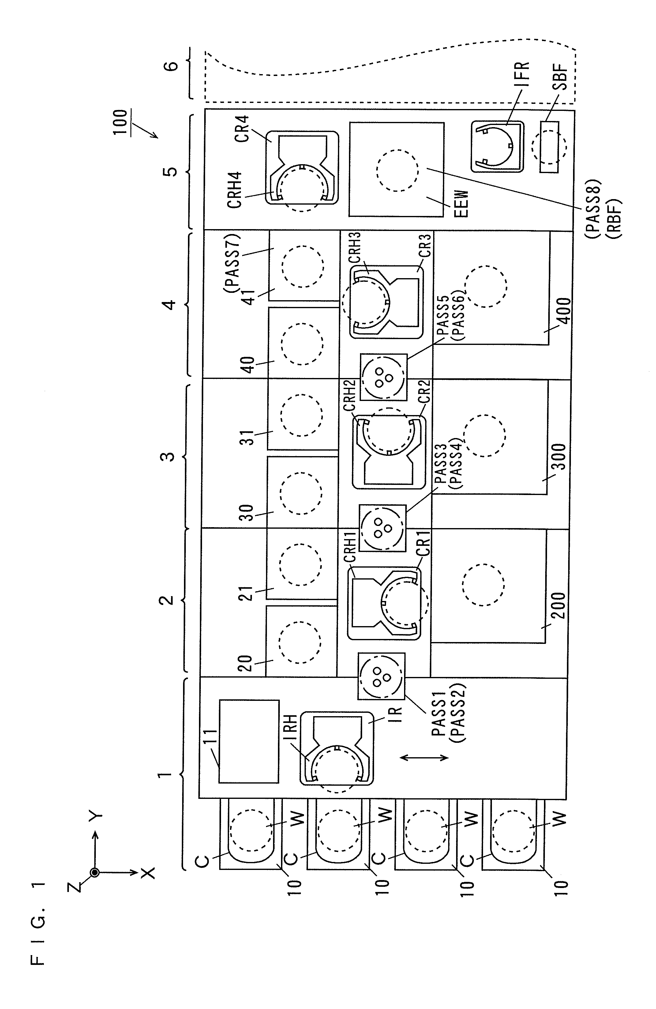
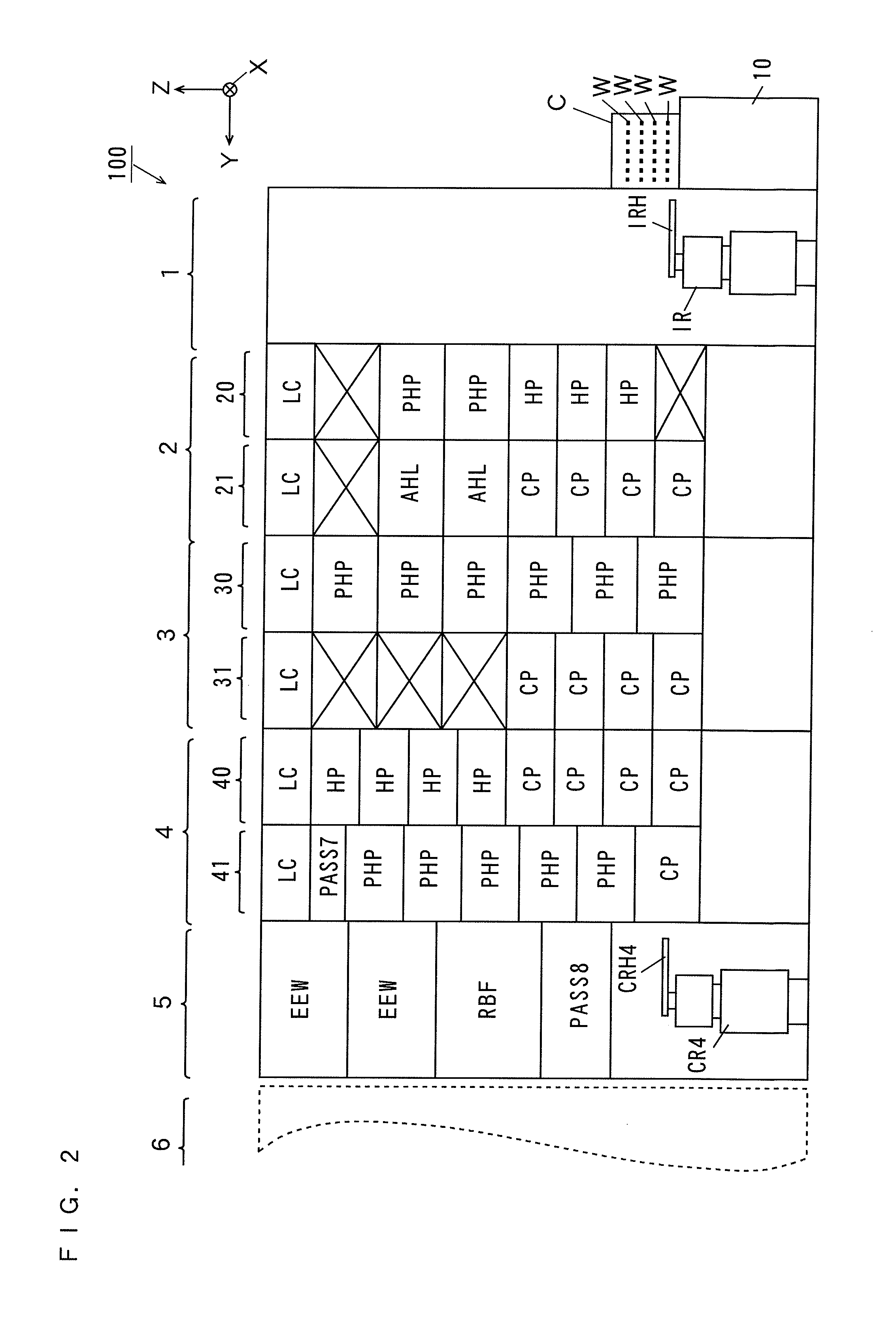
[0071](1) Configuration of the Substrate Processing Apparatus

[0072]FIG. 1 is a plan view of the substrate processing apparatus according to one...


PUM


Abstract

A substrate rotates, and a liquid nozzle of a gas / liquid supply nozzle moves to a position above the center of the rotating substrate. In this state, a rinse liquid is discharged from the liquid nozzle onto the rotating substrate. The gas / liquid supply nozzle moves toward a position outside the substrate. A gas nozzle reaches the position above the center of the rotating substrate, so that the gas / liquid supply nozzle temporarily stops. With the gas / liquid supply nozzle stopping, an inert gas is discharged onto the center of the rotating substrate for a given period of time. After that, the gas / liquid supply nozzle again moves toward the position outside the substrate.

Description

BACKGROUND OF THE INVENTION[0001]1. Field of the Invention[0002]The present invention relates to a substrate cleaning method and a substrate cleaning device for subjecting a substrate to predetermined processing.[0003]2. Description of the Background Art[0004]In photolithographic processes in manufacturing processes of semiconductor devices, liquid crystal displays and so on, resist films are first formed on substrates. The resist films formed on the substrates are subsequently exposed in predetermined patterns. The substrates that have been subjected to exposure processing are then subjected to development processing, so that resist patterns are formed on the substrates.[0005]A developing device is used for performing the foregoing development processing. The developing device includes a spin chuck that horizontally holds the substrate and rotates the substrate around an axis in a top-to-bottom direction, a developing liquid nozzle that supplies a developing liquid to the substrate...

Claims


Application Information

Patent Timeline
Patent Type & Authority Applications(United States)
IPC IPC(8): B08B3/00
CPCH01L21/67028H01L21/02052H01L21/67051H01L21/302
Inventor MIYAGI, TADASHIHARUMOTO, MASAHIKOSUYAMA, SADAYASU
Owner SCREEN SEMICON SOLUTIONS CO LTD
Why Eureka
Try Eureka