Light emitting device and method of manufacturing the light emitting device

a technology of light emitting devices and light emitting devices, which is applied in the direction of solid-state devices, semiconductor devices, coatings, etc., can solve the problems of poor processing accuracy of substrates and unsuitable for down-sizing, and achieve the effect of improving light extracting efficiency and good manufacturing yield

Active Publication Date: 2012-01-26
NICHIA CORP
View PDF8 Cites 60 Cited by
  • Summary
  • Abstract
  • Description
  • Claims
  • Application Information

AI Technical Summary

Benefits of technology

[0021]The light emitting device according to the present invention is capable of preventing the light from the light emitting element from leaking out from the bo

Problems solved by technology

However, such light emitting devices essentially require a double-sided through-hole printed circuit.
Furthermore, such su

Method used


Image

  • Light emitting device and method of manufacturing the light emitting device
  • Light emitting device and method of manufacturing the light emitting device
  • Light emitting device and method of manufacturing the light emitting device

Examples


example 1

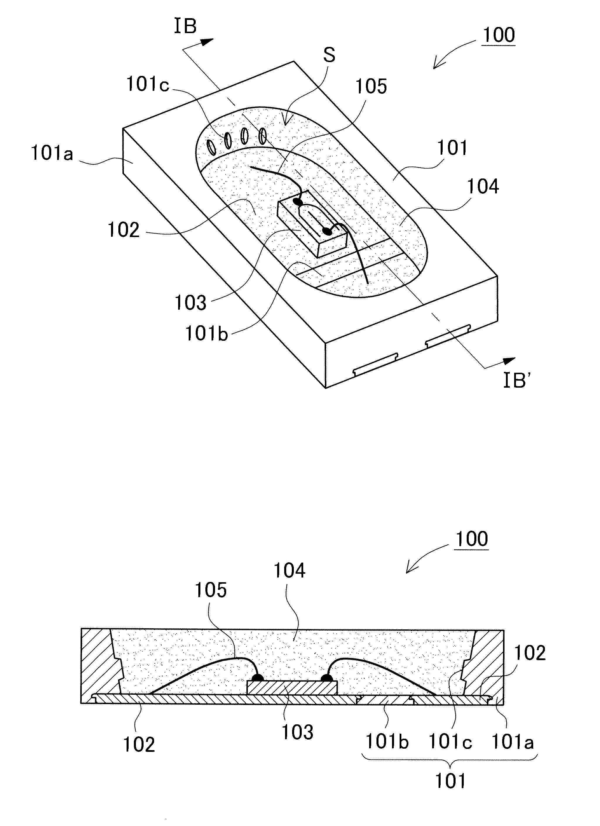
[0030]A light emitting device 100 of Example 1 is shown in FIG. 1A and FIG. 1B. FIG. 1A is a perspective view showing the light emitting device 100 and FIG. 1B is a cross-sectional view showing the light emitting device 100 shown in FIG. 1A taken along the line IB-IB′.

[0031]In Example 1, the light emitting device 100 includes, as shown in FIG. 1A and FIG. 1B, a base body 101 provided with a recess S defined by a bottom surface and a side surface, and a pair of conductive members 102 whose upper surfaces are exposed at the bottom surface of the recess S. The conductive members 102 are disposed so that its lower surface provides an outer surface of the light emitting device 100, and thus together with the base body 101, constitute a part of the lower surface of the light emitting device 100. In the recess S, a light emitting element 102 is mounted by using a bonding member (not shown) and is electrically connected to the respective conductive members 102 by a conductive wire 105 or th...

example 2

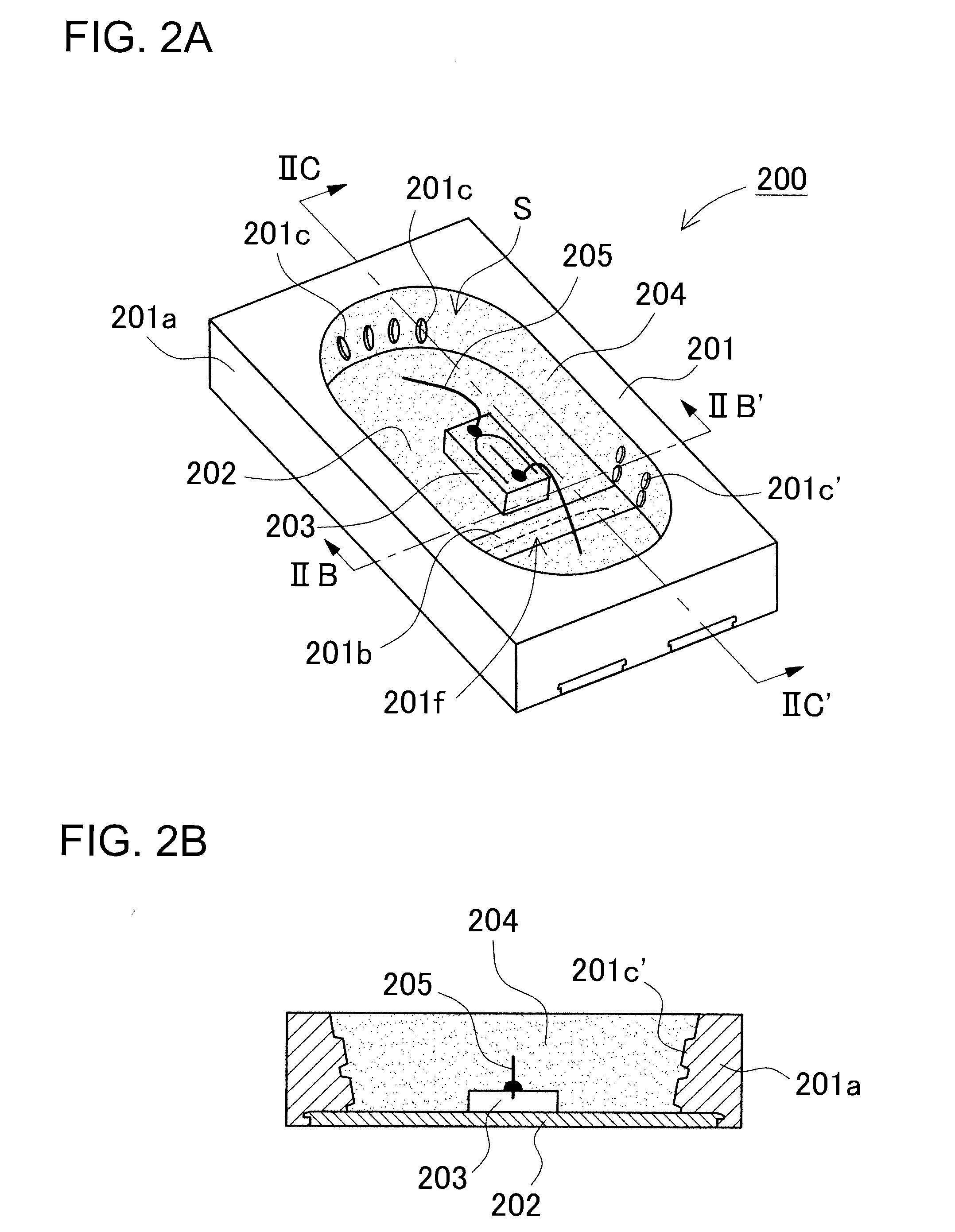
[0114]Example 1 described above illustrated an example in which the protruding portion is disposed at the shorter side of an inner surface of the side wall. However, the protruding portion can be disposed at the longer side instead of at the shorter side or in addition to the shorter side. As Example 2, such examples will be shown in FIG. 2A to FIG. 2C. In those figures, FIG. 2A is a perspective view showing a light emitting device 200 of Example 2, FIG. 2B is a cross sectional view taken along line IIB-IIB′ of FIG. 2A, and FIG. 2C is a cross-sectional view taken along line IIC-IIC′ of FIG. 2A, respectively. The light emitting devices 200 shown in FIG. 2A to FIG. 2C and the light emitting device 100 shown in FIG. 1 have the reference numerals denoted to each of the members in which the last two digits correspond to the same members, and therefore, detailed description on each members of the light emitting device 200 shown in FIG. 2 will be omitted appropriately.

[0115]The base body 2...


PUM

PropertyMeasurementUnit
Angleaaaaaaaaaa
Electrical conductoraaaaaaaaaa
Heightaaaaaaaaaa

Abstract

A light emitting device includes a base body forming a recess defined by a bottom surface and a side wall thereof, a conductive member whose upper surface being exposed in the recess and whose lower surface forming an outer surface, a protruding portion disposed in the recess, a light emitting element mounted in the recess and electrically connected to the conductive member, and a sealing member disposed in the recess to cover the light emitting element. The base body has a bottom portion and a side wall portion integrally formed of a resin, an inner surface of the side wall portion is the side wall defining the recess and has a curved portion, and the protruding portion is disposed in close vicinity to the curved surface. With this arrangement, a thin and small-sized light emitting device excellent in light extraction efficiency and reliability can be obtained.

Description

BACKGROUND OF THE INVENTION[0001]1. Technical Field[0002]The present invention relates to a resin package and a method of manufacturing the resin package, which is usable for a light emitting device applicable to image apparatus, lighting equipment, display, backlight source for liquid crystal display, or the like, and particularly to the resin package of thin and small type with high reliability, the light emitting device using the resin package and a method of manufacturing the light emitting device.[0003]2. Background Art[0004]In compliance with the recent trend of reducing the size and weight of electronic devices, there have been developed various kinds of small sized light emitting devices (light emitting diodes) to be mounted on such an electronic device. Those light emitting devices employ, for example, a double-sided through-hole printed circuit board including an insulating substrate with a pair of metallic conductive patterns formed on each of the both sides of the insula...

Claims


Application Information

Patent Timeline
IPC IPC(8): H01L33/52B05D5/12B29C45/14H01L33/62H05K1/03
CPCH01L33/486H01L33/52H01L33/60H01L2224/48091H01L2224/48247H05K5/0091H01L2224/48465H01L2924/3011H01L2924/01322H01L2924/3025H01L2924/00014H01L2924/00H01L2224/48257H01L2924/181H01L2924/00012H01L2924/18301H01L33/483H01L33/62
Inventor NISHIJIMA, SHINJIMIKI, TOMOHIDETAMAKI, HIROTO
Owner NICHIA CORP
Why Eureka
Try Eureka