Methods of forming semiconductor elements using micro-abrasive particle stream

a technology of micro-abrasive particles and semiconductor elements, applied in the field of packaging of micro-electronic devices, can solve the problems of increasing the amount of silicon, increasing the cost of each chip, and conventional methods of forming tsv holes, e.g., wet etching, etc., and can be relatively time-consuming and expensiv

Active Publication Date: 2012-01-26
TESSERA INC
View PDF12 Cites 145 Cited by
  • Summary
  • Abstract
  • Description
  • Claims
  • Application Information

AI Technical Summary

Benefits of technology

[0031]Further aspects of the invention provide systems which incorporate microelectronic structures according to the foregoing aspects of the invention, composite chips according to the foregoing aspects of the invention, or both in conjunction with o

Problems solved by technology

Such a reduction in the available space on the first face that can be used for active circuitry may increase the amount of silicon required to produce each semiconductor chip, thereby potentially increasing the cost

Method used


Image

  • Methods of forming semiconductor elements using micro-abrasive particle stream
  • Methods of forming semiconductor elements using micro-abrasive particle stream
  • Methods of forming semiconductor elements using micro-abrasive particle stream

Examples


Embodiment Construction

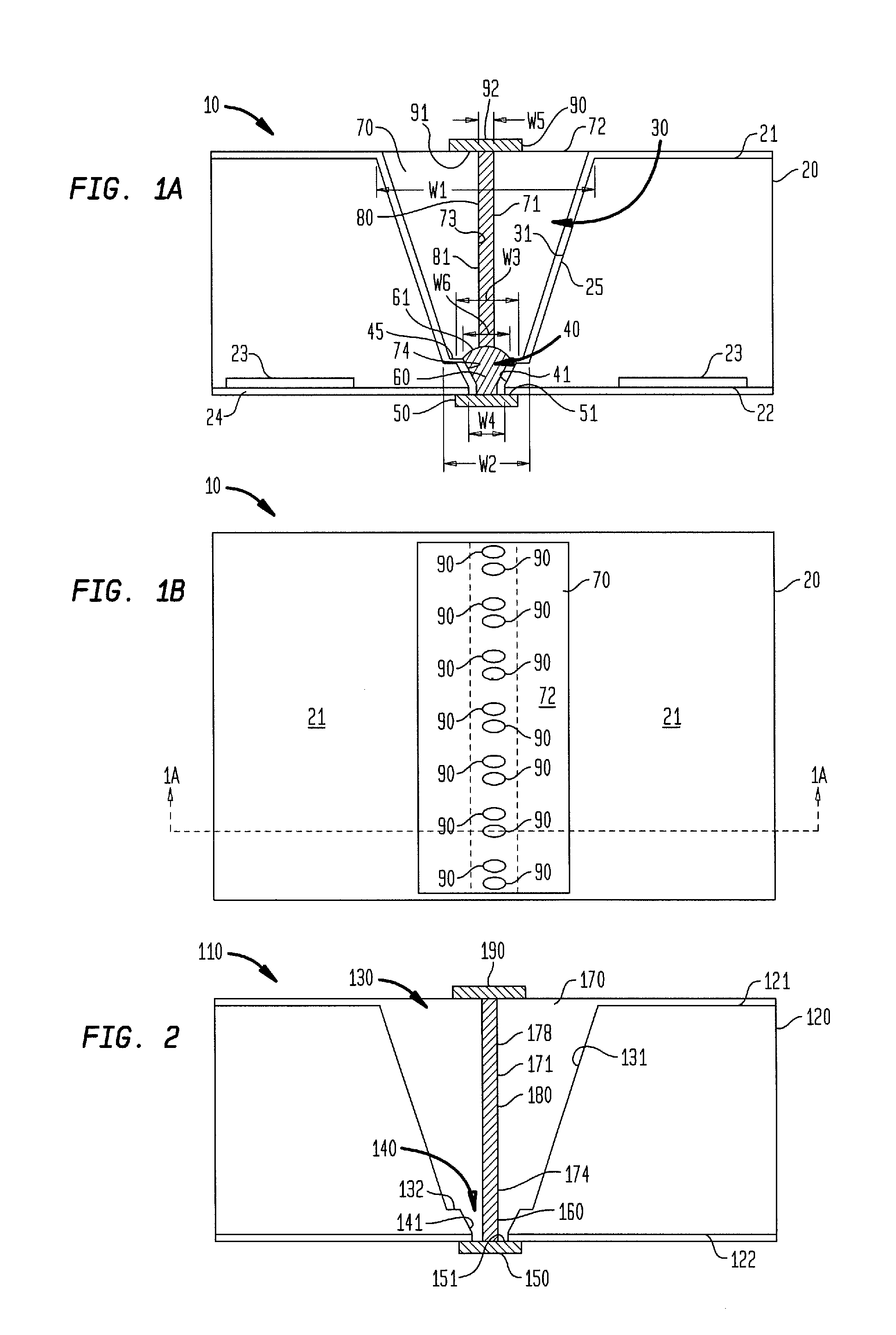
[0058]In the embodiments shown and described herein, some or all of the openings in the semiconductor element are formed by directing a jet of fine abrasive particles onto a surface of the semiconductor element. The fine abrasive particles remove material exposed at the surface. As used herein, sandblasting means this process, whether or not the abrasive particles include sand or silicon dioxide particles, a main component of sand. Use of sandblasting to form some of the openings in a semiconductor element can reduce the time and cost of producing microelectronic units, while still permitting tight opening tolerances at the active face of a semiconductor element.

[0059]FIGS. 1A and 1B are a sectional view and a corresponding top-down plan view illustrating an example via structure that can be formed in accordance with an embodiment of the invention. In the embodiment shown in FIGS. 1A and 1B, sandblasting can be used to form one or more of the openings in the semiconductor element. M...


PUM

PropertyMeasurementUnit
Timeaaaaaaaaaa
Timeaaaaaaaaaa
Angleaaaaaaaaaa

Abstract

A method of fabricating a microelectronic unit includes providing a semiconductor element having a front surface and a rear surface remote from the front surface, forming at least one first opening extending from the rear surface partially through the semiconductor element towards the front surface by directing a jet of fine abrasive particles towards the semiconductor element, and forming at least one conductive contact and at least one conductive interconnect coupled thereto. The semiconductor element can include a plurality of active semiconductor devices therein. The semiconductor element can include a plurality of conductive pads exposed at the front surface. Each conductive interconnect can extend within one or more of the first openings and can be coupled directly or indirectly to at least one of the conductive pads. Each of the conductive contacts can be exposed at the rear surface of the semiconductor element for electrical connection to an external device.

Description

BACKGROUND OF THE INVENTION[0001]The present invention relates to packaging of microelectronic devices, especially the packaging of semiconductor devices.[0002]Microelectronic elements generally comprise a thin slab of a semiconductor material, such as silicon or gallium arsenide, commonly called a die or a semiconductor chip. Semiconductor chips are commonly provided as individual, prepackaged units. In some unit designs, the semiconductor chip is mounted to a substrate or chip carrier, which is in turn mounted on a circuit panel, such as a printed circuit board.[0003]The active circuitry is fabricated in a first face of the semiconductor chip (e.g., a front surface). To facilitate electrical connection to the active circuitry, the chip is provided with bond pads on the same face. The bond pads are typically placed in a regular array either around the edges of the die or, for many memory devices, in the die center. The bond pads are generally made of a conductive metal, such as cop...

Claims


Application Information

Patent Timeline
IPC IPC(8): H01L21/768H01L23/522
CPCB24C1/045B24C3/322H01L2924/0002H01L2924/00014H01L2924/10329H01L21/76898H01L23/481H01L23/4985H01L24/03H01L24/05H01L24/06H01L2224/03464H01L2224/05009H01L2224/0557H01L2224/05624H01L2224/05647H01L2224/05666H01L2224/06181H01L2924/01013H01L2924/01029H01L2924/01033H01L2924/01061H01L2924/01079H01L2924/01082H01L2924/014H01L2924/1433H01L2924/1434H01L2924/01005H01L2924/01006H01L2924/01023H01L2924/01047H01L2924/01076H01L2224/05552H01L2924/14H01L2924/00H01L23/48
Inventor OGANESIAN, VAGEMOHAMMED, ILYASMITCHELL, CRAIGHABA, BELGACEMSAVALIA, PIYUSH
Owner TESSERA INC
Why Eureka
Try Eureka