
Patsnap Eureka
For R&D, Patsnap Eureka makes reading and utilizing patents & technical documents easy.
Patsnap Eureka AIR
Designed for self-driven R&D workflows. Generate viable solutions, solve complex R&D challenges, empower your innovation with AI.

Patsnap Eureka Materials
Designed for material experts only. Revolutionize your material R&D, from search, analyze, to developing new materials.

TechResearch
Generate reliable direction feasibility study reports for your R&D in just a few steps.

TechSeek
Discover and master advanced knowledge NOW. Basics, ideas, possibilities, all at once.

TechMind
As an expert in R&D Theories, TechMind can generates customized viable solutions instantly.

TechRisk
Analyze your overall solution with one click, know your potential R&D risks in advance.

TechMonitor
Get weekly tech updates, stay abreast of the latest tech innovations and key insights.
Solid-State Imaging Device
a solid-state imaging and imaging device technology, applied in the direction of radio-controlled devices, television system scanning details, television systems, etc., can solve the problems of inability to accurately measure the inflection point px, the inability to perform image processing with high accuracy, and the inability to accurately trace the photoelectric conversion characteristics of dummy pixels. , to achieve the effect of accurately measuring the inflection point and accurately tracing the photoelectric conversion characteristics
- Summary
- Abstract
- Description
- Claims
- Application Information
AI Technical Summary
Benefits of technology
Problems solved by technology
Method used
Image

Examples
first embodiment
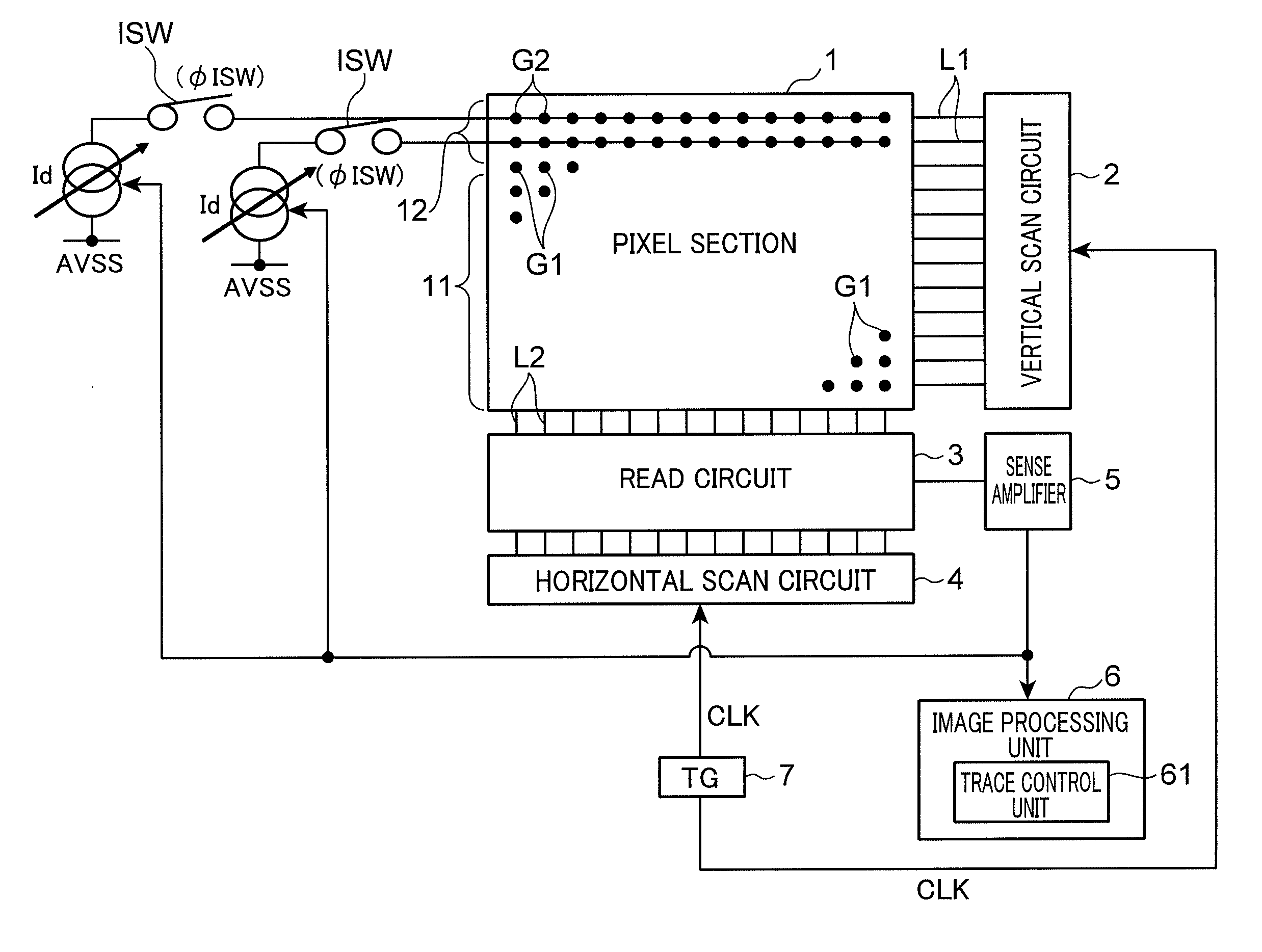
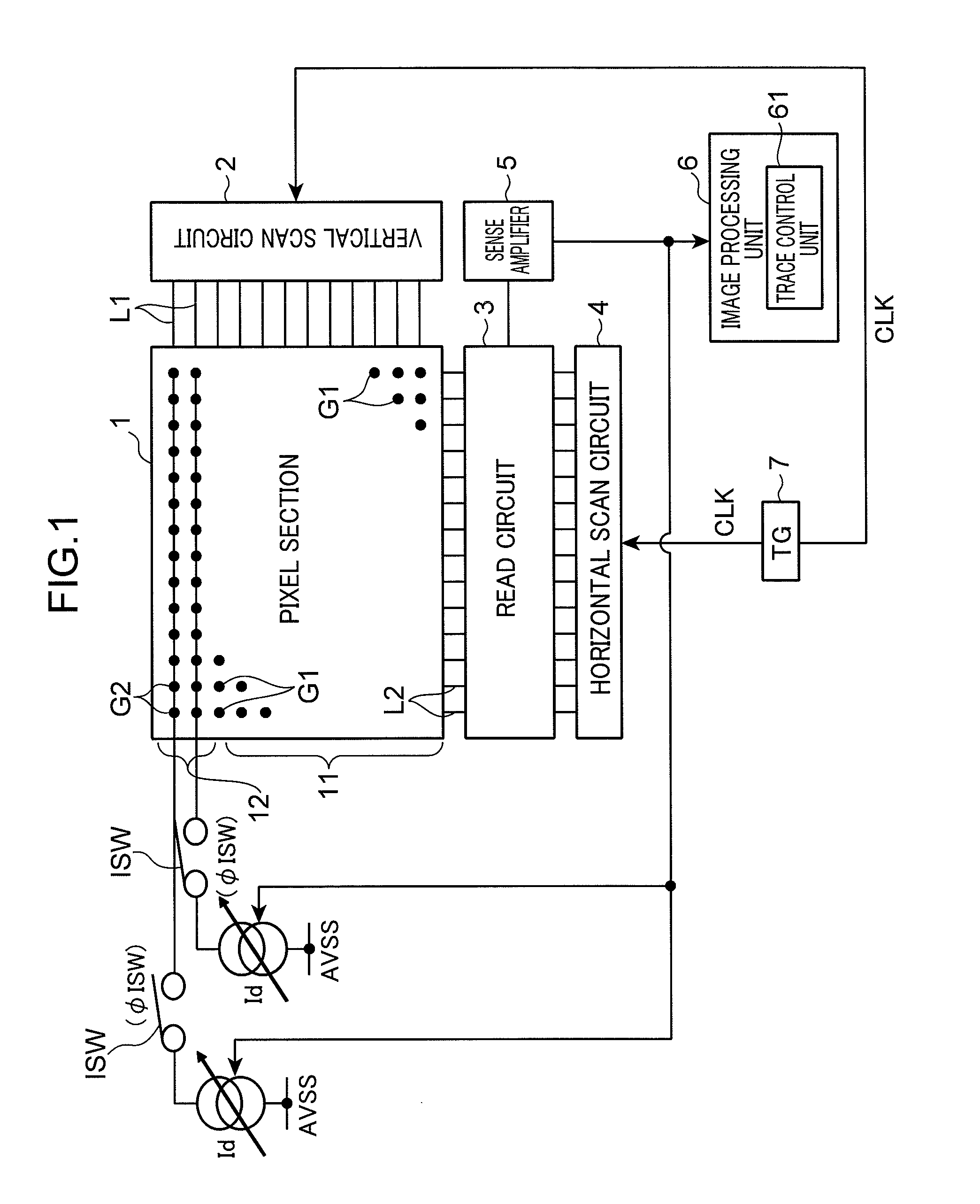
[0038]FIG. 1 shows an overall configuration diagram of a solid-state imaging device according to a first embodiment of the present invention. The solid-state imaging device is constituted by, for example, a column ADC CMOS image sensor and comprises an pixel section 1, a vertical scan circuit 2, a read circuit 3, a horizontal scan circuit 4, a sense amplifier 5, an image processing unit 6, a timing generator (TG) 7, and a constant current source Id. Moreover, the image processing unit 6 includes a trace control unit 61. The trace control unit 61 and the vertical scan circuit 2 constitute a tracing unit.
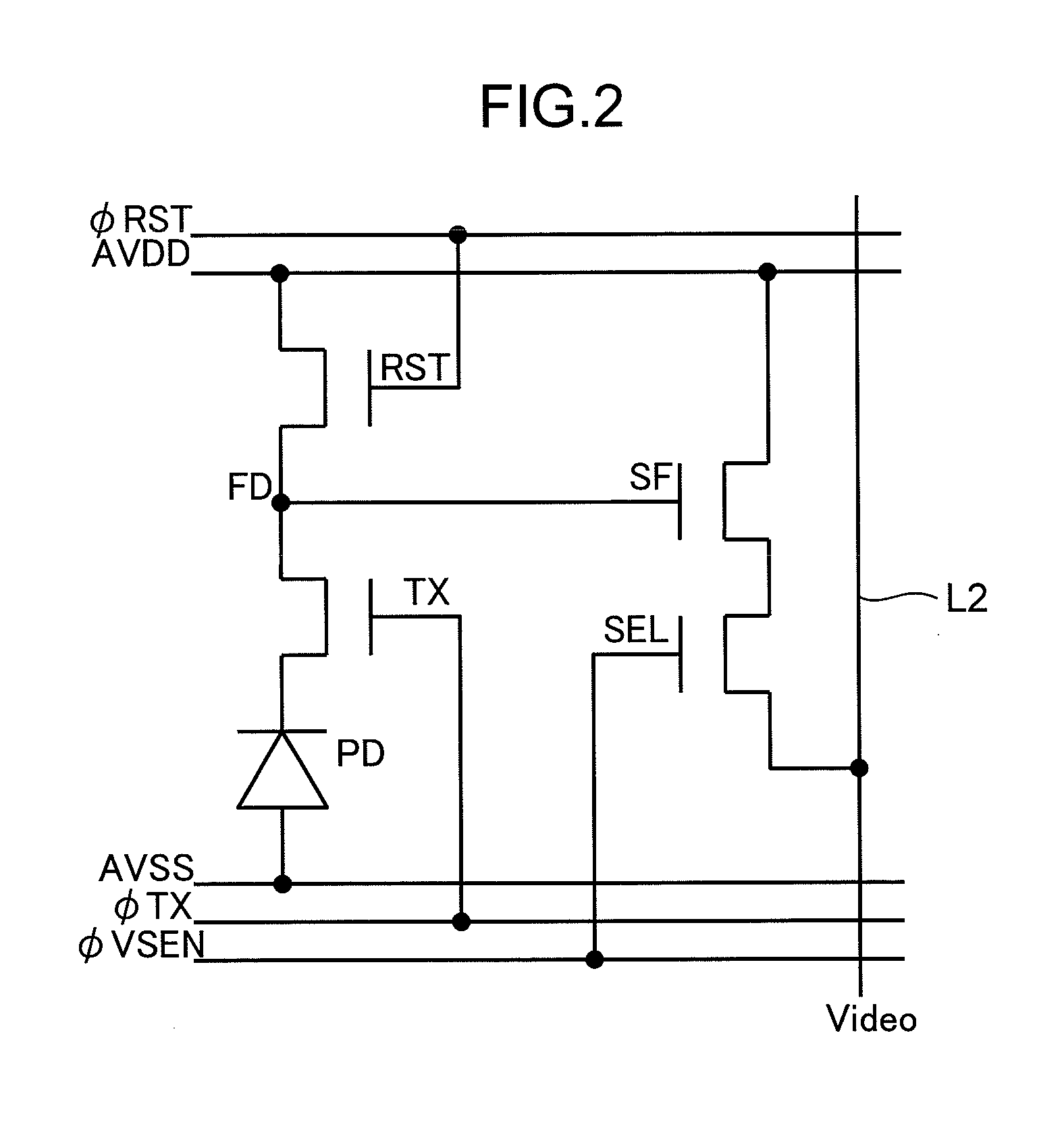
[0039]The pixel section 1 comprises, for example, an embedded photodiode, and includes pixels having photoelectric conversion characteristics including linear characteristics and logarithmic characteristics arranged in a matrix pattern. Specifically, the pixel section 1 comprises a normal pixel section 11 made up of normal pixels G1 for exposing a subject and a dummy pixel section 12 ...
second embodiment
[0107]With a solid-state imaging device according to a second embodiment, φRST which had been outputted to dummy pixels G2 in the first embodiment is replaced with φISW and is also outputted to a switch ISW. FIG. 9 shows an overall configuration diagram of a solid-state imaging device according to the second embodiment of the present invention. Moreover, in the present embodiment, a description of elements similar to those of the first embodiment will be omitted.
[0108]In FIG. 9, a row signal line L1 connected to the dummy pixels G2 is constituted by lines respectively transmitting φRST, φTX, and φVSEN. The line transmitting φRST is connected to a reset transistor RST of the dummy pixels G2 and also to the switch ISW.
[0109]Specifically, a line that transmits φRST of a corresponding row is connected to each constant current source Id, such as a line that transmits φRST outputted to dummy pixels G2 in a first row is connected to the constant current source Id of the first row, a line t...
PUM
 Abstract
Description
Claims
Application Information
 - R&D Engineer
- R&D Manager
- IP Professional
- Industry Leading Data Capabilities
- Powerful AI technology
- Patent DNA Extraction
Browse by: Latest US Patents, China's latest patents, Technical Efficacy Thesaurus, Application Domain, Technology Topic, Popular Technical Reports.
© 2024 PatSnap. All rights reserved.Legal|Privacy policy|Modern Slavery Act Transparency Statement|Sitemap|About US| Contact US: help@patsnap.com