Semiconductor device

a technology of semiconductors and devices, applied in the direction of inductance, fixed transformers or mutual inductance, digital transmission, etc., to achieve the effect of reducing the circuit area or mounting area and ensuring the reliability of operation

Inactive Publication Date: 2012-01-26
NEC CORP
View PDF3 Cites 70 Cited by
  • Summary
  • Abstract
  • Description
  • Claims
  • Application Information

AI Technical Summary

Benefits of technology

[0031]According to the present invention, it is possible to reduce the circuit area or mounting area of

Problems solved by technology

Such a problem is evident when a motor drive control system or

Method used


Image

  • Semiconductor device
  • Semiconductor device
  • Semiconductor device

Examples


first exemplary embodiment

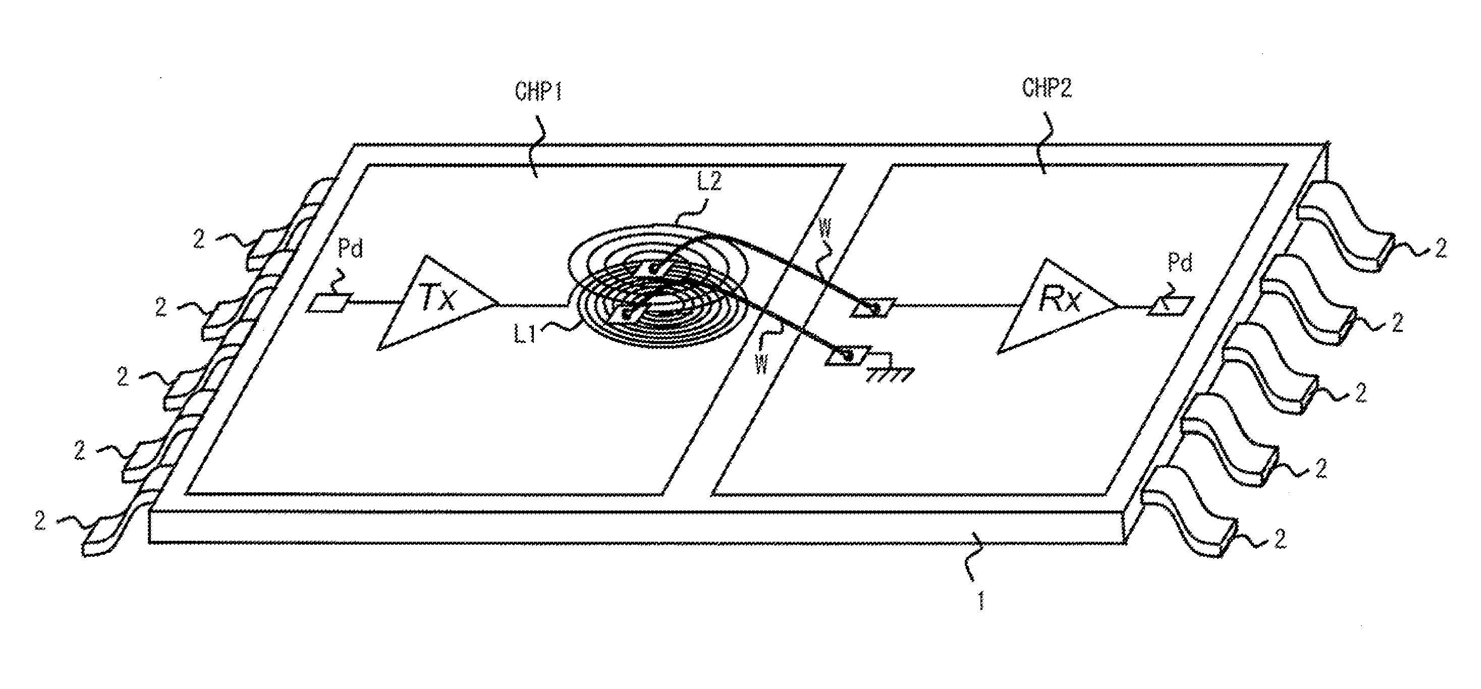
[0065]Exemplary embodiments of the present invention will be described below with reference to the drawings. FIG. 1 shows a schematic view illustrating a mounted state of a semiconductor device according to this exemplary embodiment. As shown in FIG. 1, the semiconductor device according to this exemplary embodiment includes a first semiconductor substrate CHP1 and a second semiconductor substrate CHP2. The first semiconductor substrate CHP1 and the second semiconductor substrate CHP2 are mounted in a single semiconductor package.

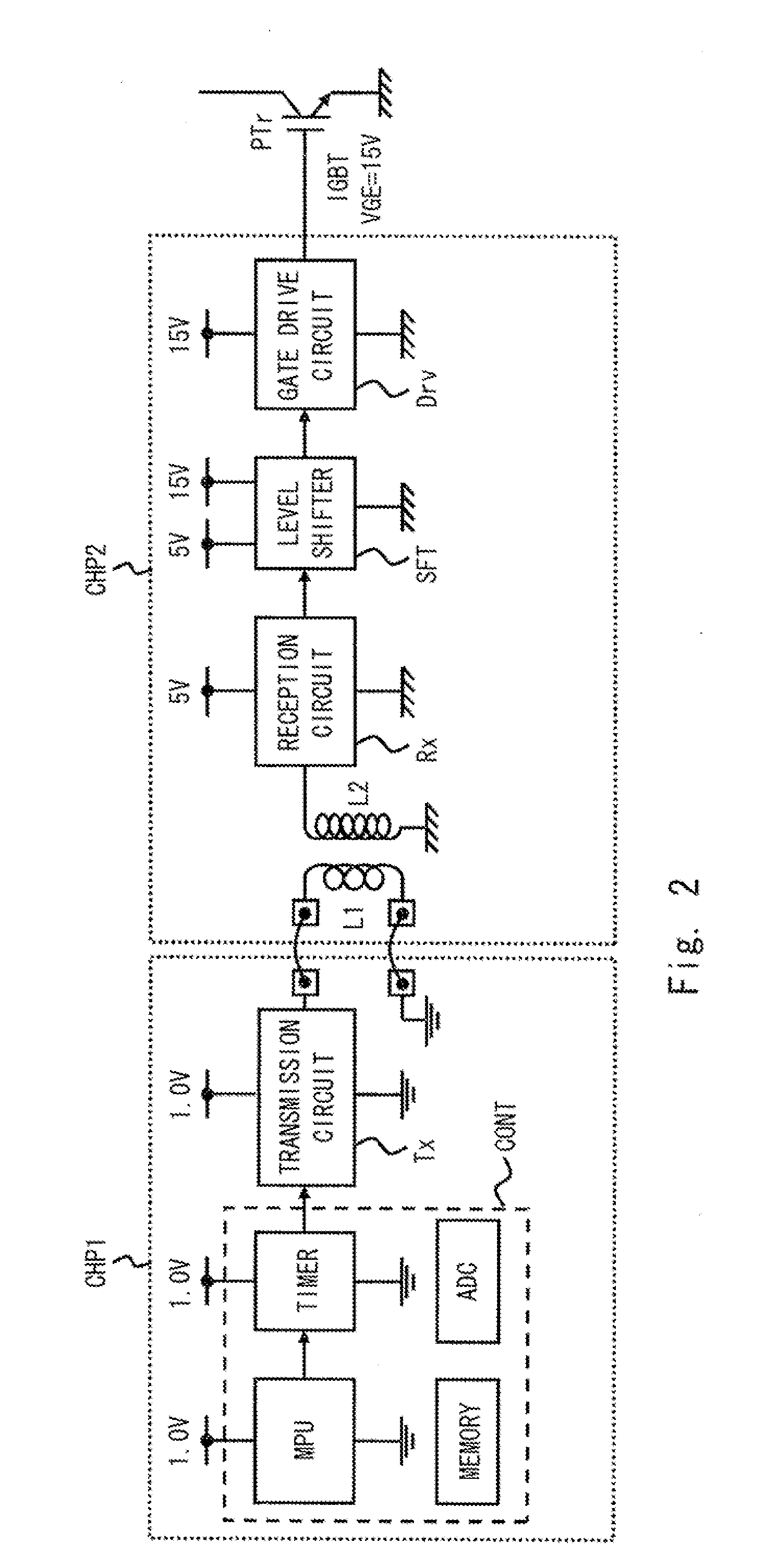
[0066]The first semiconductor substrate CHP1 includes a control circuit and a transmission circuit Tx. The second semiconductor substrate CHP2 includes a reception circuit Rx and a gate drive circuit Drv. In the example shown in FIG. 1, the second semiconductor substrate CHP2 includes an AC coupling element (for example, a transformer). The transformer includes a primary coil L1 and a secondary coil L2. The secondary coil L2 is connected to an output of the...

second exemplary embodiment

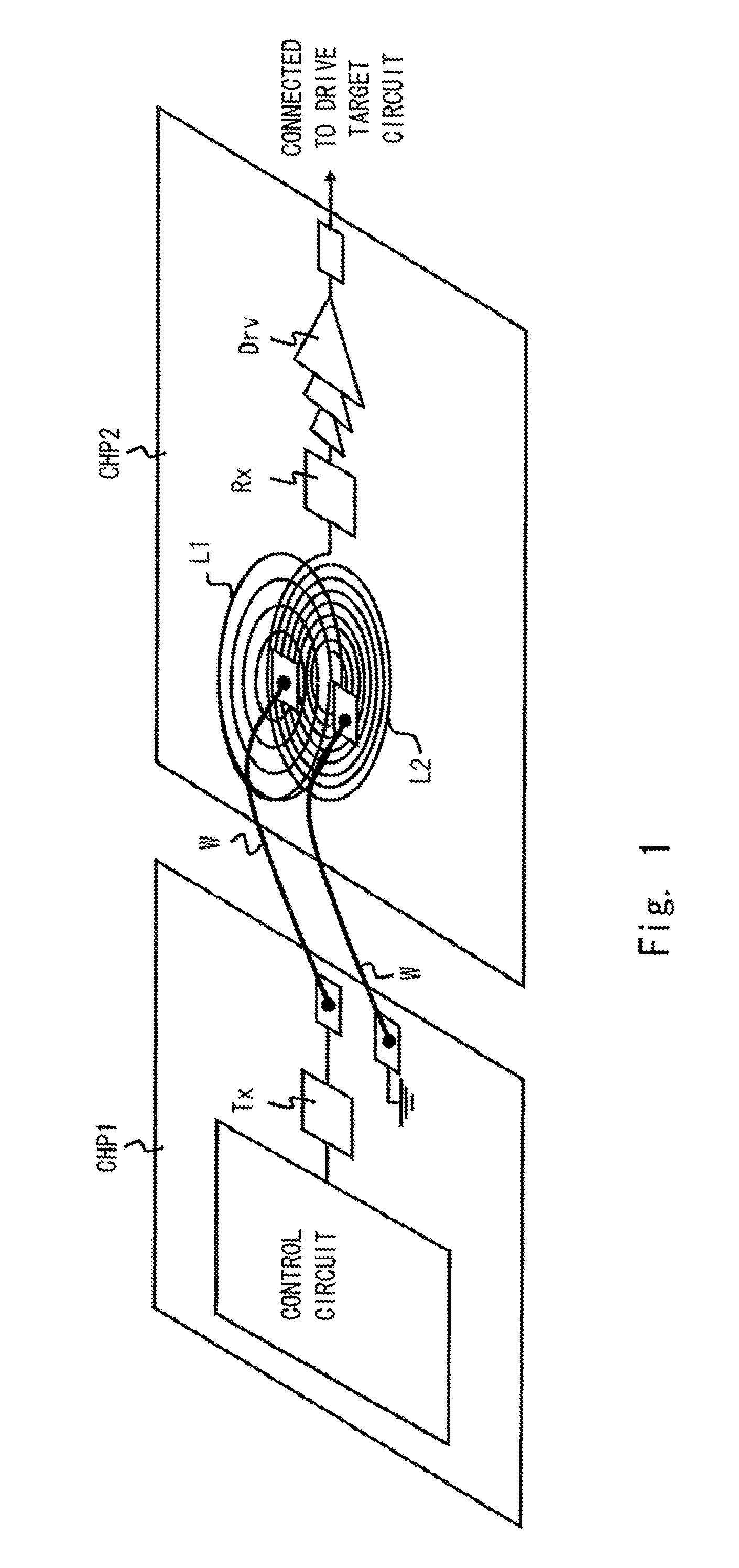
[0126]FIG. 28 shows a schematic view illustrating a mounted state of a semiconductor device according to a second exemplary embodiment. As shown in FIG. 28, the semiconductor device according to the second exemplary embodiment has a configuration in which a communication path from the second semiconductor substrate CHP2 to the first semiconductor substrate CHP1 is provided to the semiconductor device according to the first exemplary embodiment. Also in the semiconductor device according to the second exemplary embodiment, an AC coupling element (for example, a transformer) is used for communication. Also in the second exemplary embodiment, the transmission circuit Tx2 formed on the second semiconductor substrate CHP2 transmits a signal obtained by modulating a transmission signal, and the reception circuit Rx2 formed on the first semiconductor substrate CHP1 demodulates the signal output by the transmission circuit Tx2 to reproduce transmission data.

[0127]Thus, the provision of the ...


PUM


Abstract

A semiconductor device according to the present invention includes: a first semiconductor substrate CHP1 including a control circuit that generates a control signal for a control target circuit, and a transmission circuit Tx that modulates the control signal to generate a transmission signal; a second semiconductor substrate CHP2 including a reception circuit Rx that demodulates the transmission signal transmitted from the transmission circuit to reproduce the control signal, and a drive circuit Drv that drives the control target circuit based on the control signal output from the reception circuit, the second semiconductor substrate CHP2 being electrically insulated from the first semiconductor substrate CHP1; an AC coupling element that is formed on a semiconductor substrate and couples the first semiconductor substrate CHP1 and the second semiconductor substrate CHP2 in an alternating manner; and a semiconductor package 20 including the first semiconductor substrate CHP1, the second semiconductor substrate CHP2, and the AC coupling element. This suppresses an increase in circuit area or mounting area.

Description

TECHNICAL FIELD [0001]The present invention relates to a semiconductor device, and more particularly, to a semiconductor device including a first semiconductor substrate and a second semiconductor substrate which communicate with each other through an AC coupling element based on different power supply voltages.BACKGROUND ART [0002]In general, a plurality of semiconductor chips or semiconductor packages are used to control a system incorporating a power transistor with a high breakdown voltage. In this regard, FIGS. 29 to 31 each show a block diagram of a semiconductor device that controls a power transistor PTr with a high breakdown voltage. In such a system as shown in FIGS. 29 to 31, a control circuit 101, which generates a control signal for the power transistor PTr, and a gate drive circuit 103, which drives the power transistor PTr, are connected via an insulating interface 102.[0003]In order to adjust electric energy supplied to an electric motor, lighting equipment, or the l...

Claims


Application Information

Patent Timeline
IPC IPC(8): H04L27/00
CPCH01F19/08H01F2017/0086H01F2019/085H04L25/4902H01L2224/48091H01L2224/48137H01L2924/13091H01L2224/49175H01L2924/13055H01L2924/30107H01L2924/3011H01L2924/1305H01L2924/00014H01L2924/00H01L2224/05553H01L2224/05554H01L2224/0603H01L2224/45099
Inventor KAERIYAMA, SHUNICHI
Owner NEC CORP
Why Eureka
Try Eureka