Multilayer wiring substrate

a wiring substrate and multi-layer technology, applied in the direction of printed circuit manufacturing, printed circuit stress/warp reduction, printed circuit aspects, etc., can solve the problems of difficult bonding of ic chips directly onto the motherboard, circuitry malfunction, and hindering the implementation of high operation speed, etc., to achieve the effect of improving yield, improving reliability and relatively easy manufacturing

Inactive Publication Date: 2012-02-02
NGK SPARK PLUG CO LTD
View PDF0 Cites 24 Cited by
  • Summary
  • Abstract
  • Description
  • Claims
  • Application Information

AI Technical Summary

Benefits of technology

[0012]The present invention has been accomplished in view of the above problems, and an object of the invention is to provide a multilayer wiring substrate whose reliability is enhanced through prevention of generation of cracks in connection portions between the multilayer wiring substrate, and an IC chip or a motherboard.
[0027]Preferably, the reinforcement member is stiffer than the resin material used to form the laminate structure. For example, the Young's modulus of the reinforcement member is desirably greater than that of the resin material used to form the laminate structure. The reason is as follows. In the case where high rigidity is imparted to the reinforcement member itself, high rigidity can be imparted to the laminate structure by means of joining the reinforcement member thereto, whereby the laminate structure becomes stronger against externally applied stress. Further, in the case where the rigidity of the reinforcement member is high, a sufficiently high rigidity can be imparted to the laminate structure even when the thickness of the reinforcement member is decreased. Thus, the reinforcement member does not hinder reduction of the overall thickness of the laminate structure.

Problems solved by technology

However, since the terminals of the IC chip differ greatly in pitch from those of the motherboard, difficulty is encountered in bonding the IC chip directly onto the motherboard.
In this case, the conductor lines which extend through the substrate core serve as sources of high inductance, leading to the transmission loss of high-frequency signals and the occurrence of circuitry malfunction and thus hindering implementation of high operation speed.
Meanwhile, a multilayer wiring substrate is formed from a resin material or the like whose overall thermal expansion coefficient is about 30 ppm / ° C. Therefore, the conventional multilayer wiring substrate is greater in thermal expansion coefficient than the IC chip, which brings about the following problem.
When solder used for connection between the IC chip and the multilayer wiring substrate is cooled, due to the influence of thermal stress stemming from the difference in thermal expansion coefficient between the material of the IC chip and the material of the multilayer wiring substrate, cracks may be generated in connection portions, and open failure or the like may occur.
That is, in the case where the multilayer wiring substrate as described above is configured, there arises a problem in that high yield and reliability cannot be realized.

Method used


Image

  • Multilayer wiring substrate
  • Multilayer wiring substrate
  • Multilayer wiring substrate

Examples


Embodiment Construction

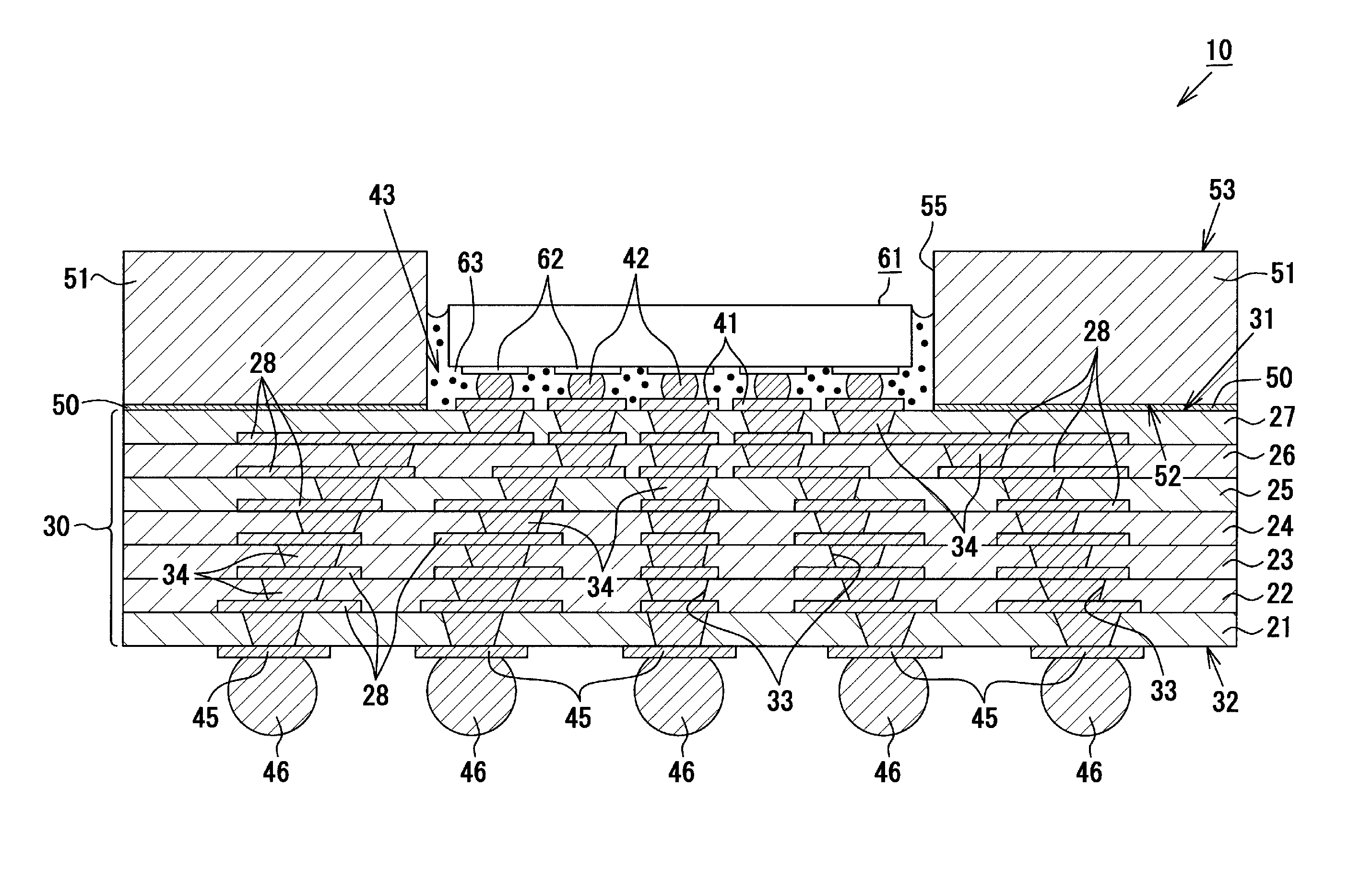
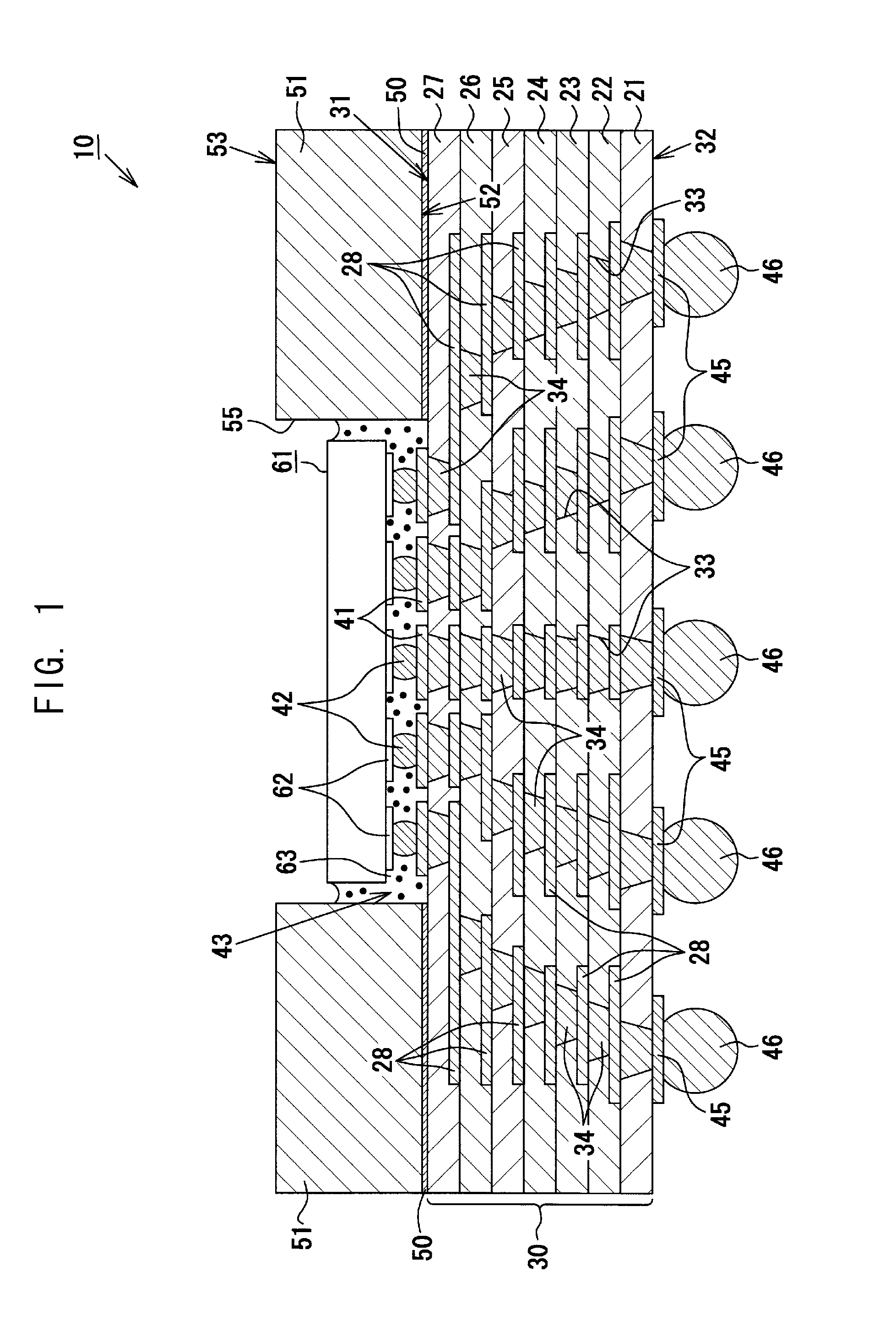
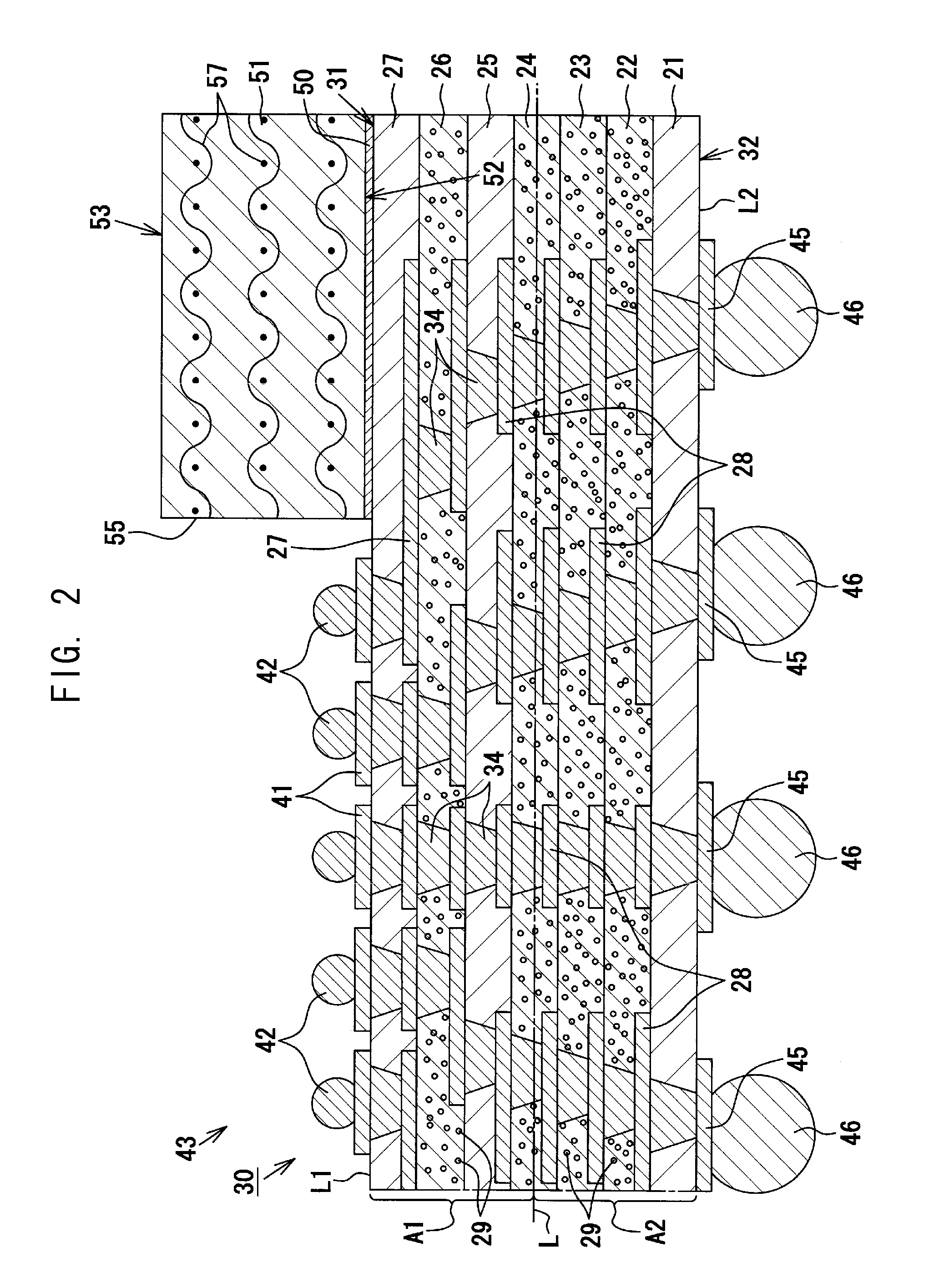
[0042]An embodiment in which a multilayer wiring substrate of the present invention is embodied will next be described in detail with reference to the drawings.

[0043]As shown in FIGS. 1 and 2, an exemplary multilayer wiring substrate 10 is a core-less wiring substrate 10 which does not include a substrate core, and includes a wiring laminate portion 30 (laminate structure) having a first main face 31 (first main surface) (upper surface in FIG. 1) and a second main face 32 (second main surface) (lower surface in FIG. 1). The exemplary wiring laminate portion 30 of the present embodiment assumes a generally rectangular shape as viewed from above, and has a size of 50.0 mm (longitudinal direction)×50.0 mm (lateral direction)×0.28 mm (thickness).

[0044]The exemplary wiring laminate portion 30 has a multilayer structure in which seven resin insulation layers 21, 22, 23, 24, 25, 26, 27 and six conductor layers 28 are alternately laminated. Each of the resin insulation layers 21 to 27 is fo...


PUM

PropertyMeasurementUnit
thicknessaaaaaaaaaa
temperatureaaaaaaaaaa
sizeaaaaaaaaaa

Abstract

A multilayer wiring substrate includes a laminate structure in which resin insulation layers and conductor layers are alternately laminated. The resin insulation layers include first-type resin insulation layers, and second-type resin insulation layers, each of which contains an inorganic material in a larger amount and is smaller in thermal expansion coefficient as compared with first-type resin insulation layers. On a cross section of the laminate structure taken along a thickness direction thereof, the ratio of a total thickness of the second-type resin insulation layers located in an area A2 to a thickness corresponding to the area A2 is greater than the ratio of a total thickness of the second-type resin insulation layers located in an area A1 to a thickness corresponding to the area A1. The laminate structure is warped such that the laminate structure is convex toward the side where the second main face is present.

Description

CROSS REFERENCE TO RELATED APPLICATIONS[0001]The present application claims priority from Japanese Patent Application No. 2010-173305, which was filed on Aug. 2, 2010, the disclosure of which is herein incorporated by reference in its entirety.BACKGROUND OF THE INVENTION[0002]1. Field of the Invention[0003]The present invention relates to a multilayer wiring substrate having a laminate structure in which a plurality of resin insulation layers and a plurality of conductor layers are laminated alternately in multilayer arrangement, and not having a so-called substrate core in a final product, the substrate core carrying build-up layers successively formed on opposite surfaces thereof.[0004]2. Description of Related Art[0005]In association with recent increasing tendency toward higher operation speed and higher functionality of IC chips used as, for example, microprocessors of computers, the number of terminals increases, and the pitch between the terminals tends to become narrower. Ge...

Claims


Application Information

Patent Timeline
Patent Type & Authority Applications(United States)
IPC IPC(8): H05K1/00
CPCH01L21/4857H01L23/145H01L2924/15311H01L2224/73204H01L2224/32225H01L2224/16225H05K2203/041H05K2201/2009H05K2201/10977H05K3/4688H01L23/49816H01L23/49822H01L23/49833H01L2924/09701H05K1/0271H05K3/4015H05K3/4682H01L2924/00H01L23/32H01L23/12H01L23/52H01L23/48
Inventor MAEDA, SHINNOSUKEHIRANO, SATOSHI
Owner NGK SPARK PLUG CO LTD
Why Eureka
Try Eureka