Electron detector including an intimately-coupled scintillator-photomultiplier combination, and electron microscope and x-ray detector employing same

a scintillator and photomultiplier technology, applied in the field of electron microscope and x-ray detectors, can solve the problems of significant reduction in the light collection efficiency for otherwise, the requirement for very small and very thin samples, and the cost of such a small and thin sample,

Active Publication Date: 2012-02-02
FEI CO
View PDF14 Cites 64 Cited by
  • Summary
  • Abstract
  • Description
  • Claims
  • Application Information

AI Technical Summary

Problems solved by technology

Their disadvantages are their cost and the requirement for very small and very thin samples.
The light guide and its attachment to the scintillator, however, play an important role in determining the device performance, and its required presence cannot be ignored.
This results in a significant reduction in light collection efficiency for otherwise optimum BSED geometries.
A further implication is that the light generated on the side of the scintillator disk opposite the light guide is not effectively transmitted to the PMT, meaning that there is always a topographical bias in the image (the view from one side of the column centerline dominates the image).
In spite of this important capability, scintillator-based devices are often chosen over segmented photodiode detectors because they have much higher gain and can image at much faster scanning rates; in this case, the advantage of the selection of topographic or compositional modes provided by the photodiode detector is lost.
Furthermore, the MCP is slow and shares the disadvantage with the photodiode detector that it is unable to keep pace with the very short dwell times (high scanning rates) used in modern SEMs.

Method used


Image

  • Electron detector including an  intimately-coupled scintillator-photomultiplier combination, and electron microscope and x-ray detector employing same
  • Electron detector including an  intimately-coupled scintillator-photomultiplier combination, and electron microscope and x-ray detector employing same
  • Electron detector including an  intimately-coupled scintillator-photomultiplier combination, and electron microscope and x-ray detector employing same

Examples


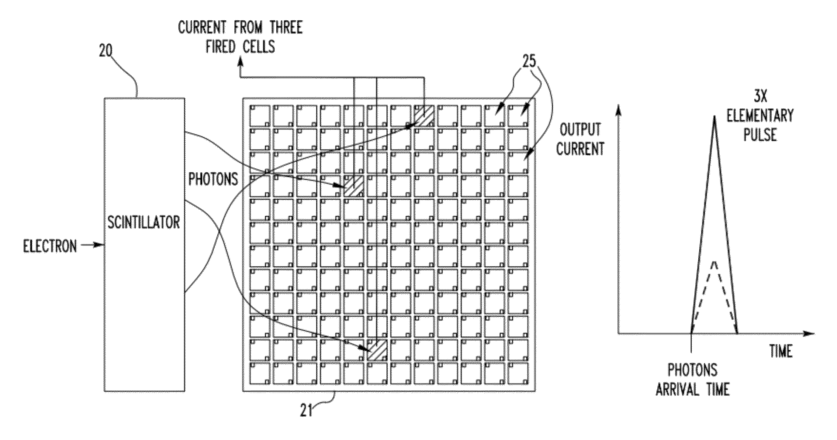
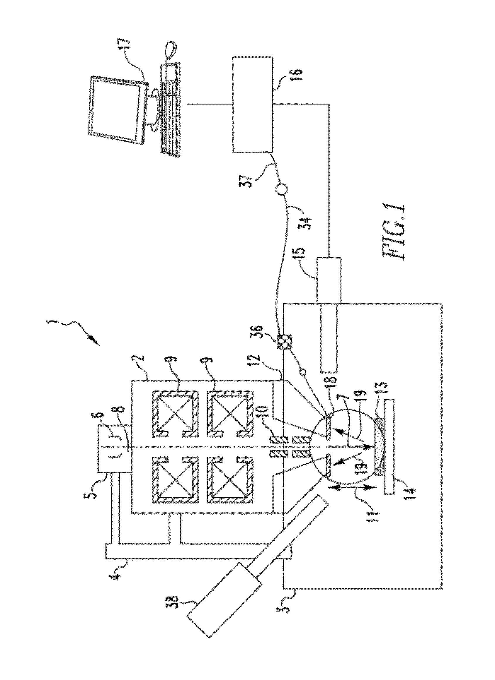
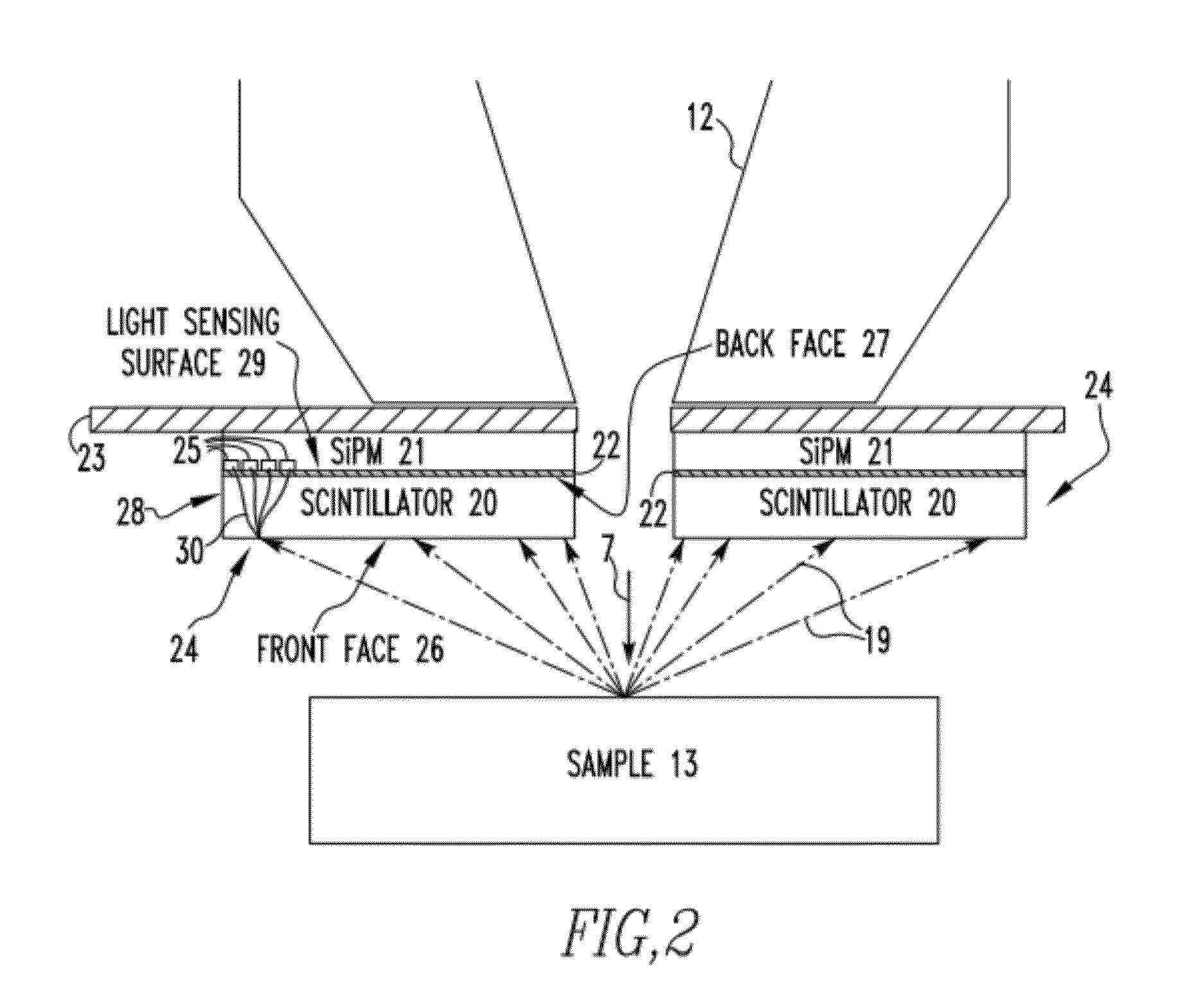
Embodiment Construction

[0050]As used herein, the singular form of “a”, “an”, and “the” include plural references unless the context clearly dictates otherwise. As used herein, the statement that two or more parts or components are “coupled” shall mean that the parts are joined or operate together either directly or indirectly, i.e., through one or more intermediate parts or components, so long as a link occurs. As used herein, “directly connected” means that two elements are either directly in contact with each other or are connected to one another by a bonding / coupling material or agent without any other intermediate elements, parts or components in between. As used herein, “fixedly coupled” or “fixed” means that two components are coupled so as to move as one while maintaining a constant orientation relative to each other. As used herein, the statement that a first item is “based on” a second item shall mean that the second item serves as a direct or indirect (such as through one or more intermediate ca...


PUM


Abstract

A charged particle beam device includes an electron source structured to generate an electron beam, the electron source being coupled to an electron column that at least partially houses a system structured to direct the electron beam toward a specimen positioned in a sample chamber to which the electron column is coupled, and an electron detector. The electron detector includes one or more assemblies positioned within the electron column or the sample chamber, each of the assemblies including an SiPM and a scintillator directly connected face-to-face to an active light sensing surface of the SiPM without a light transporting device being positioned in between the scintillator and the SiPM.

Description

CROSS-REFERENCE TO RELATED APPLICATIONS[0001]This application claims priority under 35 U.S.C. §119(e) from U.S. Provisional Application No. 61 / 369,353 entitled “Electron Microscope Employing An SiPM Based Electron Detector” and filed on Jul. 30, 2010, the disclosure of which is incorporated herein by reference.BACKGROUND OF THE INVENTION[0002]1. Field of the Invention[0003]The present invention pertains to electron detection and electron detection devices, and, in particular, to an electron detector including an intimately-coupled scintillator-silicon photomultiplier combination that may be employed in an electron microscope and / or an X-ray detector, such as an X-ray detector used in an electron microscope.[0004]2. Description of the Related Art[0005]An electron microscope (EM) is a type of microscope that uses a particle beam of electrons to illuminate a specimen and produce a magnified image of the specimen. One common type of EM is known as a scanning electron microscope (SEM). A...

Claims


Application Information

Patent Timeline
Patent Type & Authority Applications(United States)
IPC IPC(8): H01J37/26G01T1/20G01T1/24
CPCG01T1/2018H01J37/244G01N23/2257H01J2237/24415H01J2237/2443H01J37/28G01T1/20185G01T1/20188
Inventor BARBI, NICHOLAS C.LOPOUR, FILIPPIEDMONTE, CLAUDIOMOTT, RICHARD B.
Owner FEI CO
Why Eureka
Try Eureka