

Design apparatus of semiconductor device, design method of semiconductor device, and semiconductor device
- Summary
- Abstract
- Description
- Claims
- Application Information
AI Technical Summary
Benefits of technology
Problems solved by technology
Method used
Image

Examples
Embodiment Construction
[0035]The invention will be now described herein with reference to illustrative embodiments. Those skilled in the art will recognize that many alternative embodiments can be accomplished using the teachings of the present invention and that the invention is not limited to the embodiments illustrated for explanatory purposed.
[0036]Referring to attached drawings, a design apparatus of a semiconductor, a design method of a semiconductor device, and a semiconductor device according to an embodiment of the present invention will be described below.
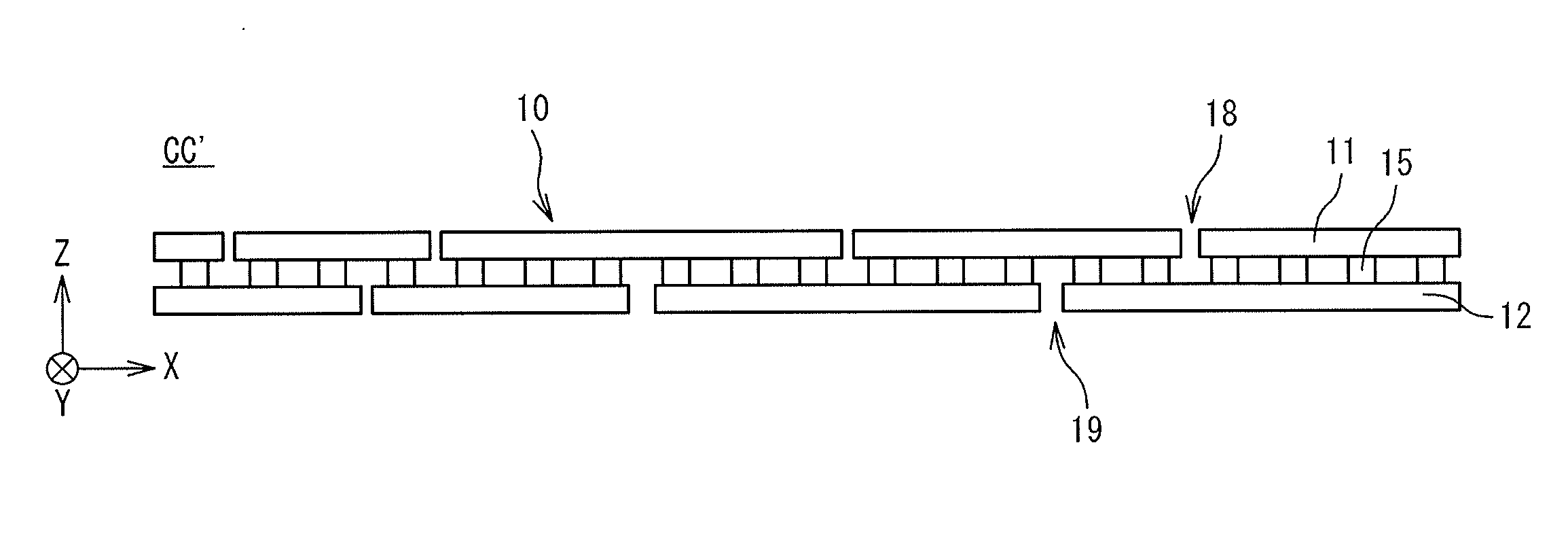
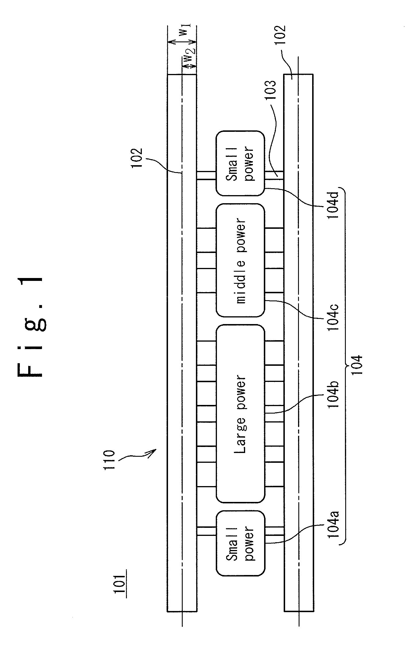
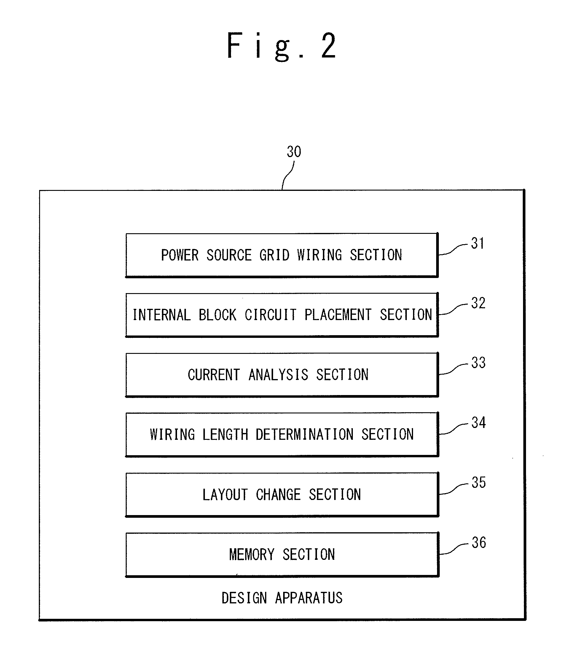
[0037]FIG. 2 is a block diagram showing a configuration of the design apparatus of the semiconductor device according to the embodiment of the present invention. The design apparatus 30 carries out a wiring design of the semiconductor device by using an automatic placement and routing tool for a semiconductor device. In the designing of wiring lines (for example, designing of a power source grid), the design apparatus 30 determines wiring lines...
PUM
 Abstract
Description
Claims
Application Information